
Sample-and-hold amplifiers

a technology of amplifiers and amplifiers, applied in amplifiers with semiconductor devices/discharge tubes, electric analogue stores, instruments, etc., can solve the problems of low voltage integrated circuits that may output wrong signals, noise usually dominates overall signal-to-noise plus distortion ratio (sndr) performan

Active Publication Date: 2010-12-07
MEDIATEK INC
View PDF8 Cites 4 Cited by
  • Summary
  • Abstract
  • Description
  • Claims
  • Application Information

AI Technical Summary

Benefits of technology

The patent describes a sample-and-hold amplifier that includes a sample-and-hold circuit, a buffer circuit, and a native MOS transistor. The sample-and-hold circuit receives an input signal and sends it to a first node based on a control signal. The buffer circuit is connected between a power supply and ground and controlled by the first node to provide an output signal at an output node. The native MOS transistor is connected to the output node and controls the output of the signal. The amplifier has a low threshold voltage, meaning it can operate with low power consumption. The voltage provided by the power supply is within a specific range. The technical effect of this invention is to provide a low-power, efficient sample-and-hold amplifier for use in various electronic devices.

Problems solved by technology

When level shifting, that is noise, occurs in a low voltage integrated circuit, the low voltage integrated circuit may output wrong signals.
Especially, for a low voltage high resolution pipelined analog-digital converter (ADC) in digital applications, noise usually dominates overall signal-to-noise plus distortion ratio (SNDR) performance.

Method used


Image

  • Sample-and-hold amplifiers
  • Sample-and-hold amplifiers
  • Sample-and-hold amplifiers

Examples


Embodiment Construction

[0016]The following description is of the best-contemplated mode of carrying out the invention. This description is made for the purpose of illustrating the general principles of the invention and should not be taken in a limiting sense. The scope of the invention is best determined by reference to the appended claims.

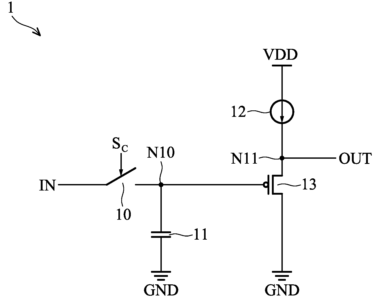
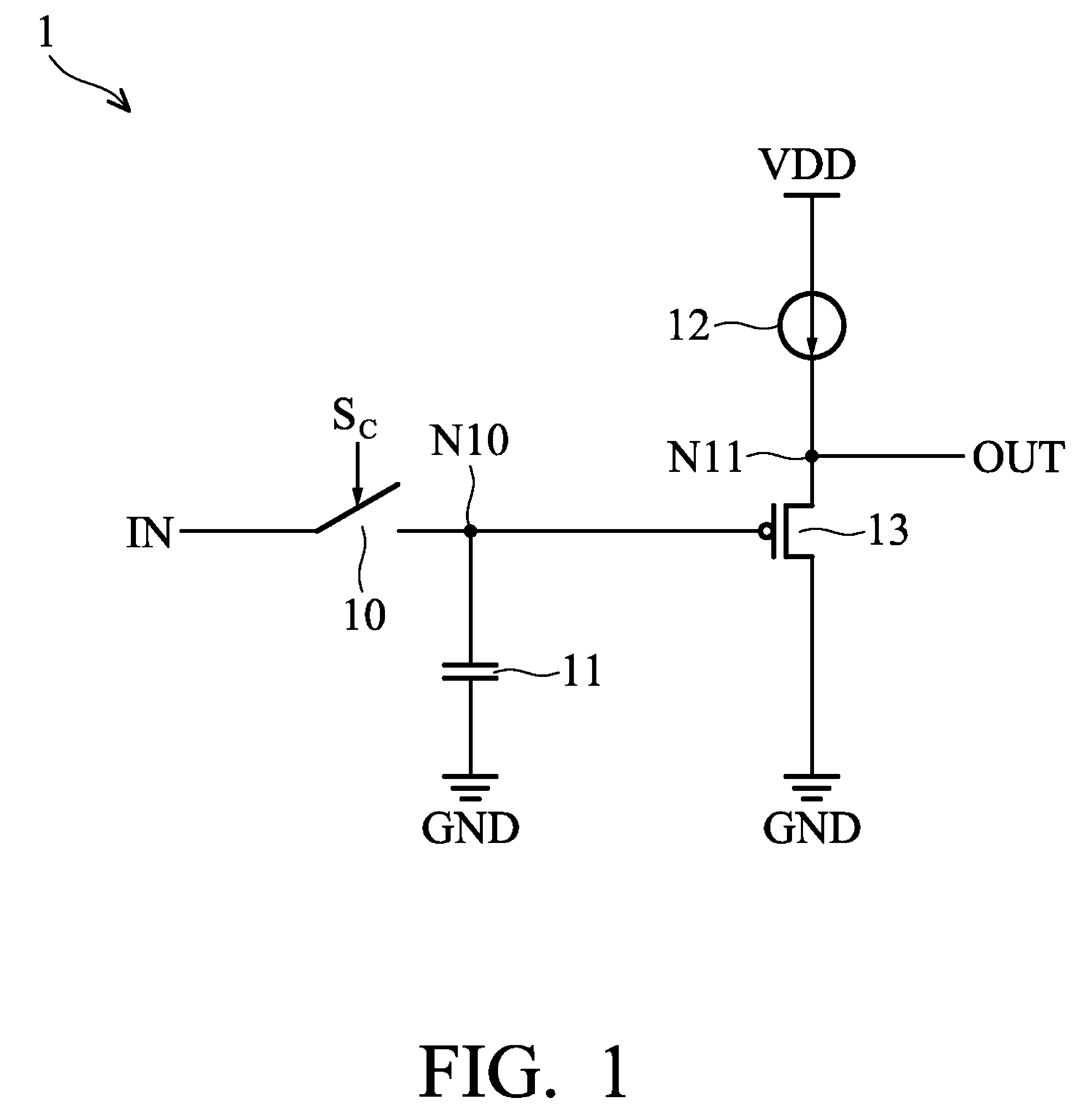
[0017]FIG. 1 shows a simple sample-and-hold amplifier. Referring to FIG. 1, the sample-and-hold amplifier 1 comprises a switch device 10, a capacitor 11, a current source 12, and a PMOS transistor 13. The switch device 10 receives an input signal IN and is controlled by a control signal SC to be turned on or off. The capacitor 11 is coupled between a node N10 and a ground GND. The PMOS transistor 13 is coupled between an output node N11 and the ground GND and controlled by the node N10. The current source 12 is coupled between a supply voltage source VDD and the output node N11 which provides an output signal OUT.

[0018]It is assumed that the sample-and-hold amplifier 1...


PUM


Abstract

A sample-and-hold amplifier is provided. The sample-and-hold amplifier comprises a sample-and-hold circuit and a buffer circuit. The sample-and-hold circuit receives an input signal and transmits the input signal to a first node according to a control signal. The buffer circuit is coupled between a supply voltage source and a ground and controlled by the first node to provide an output signal at an output node. The buffer circuit comprises a native MOS transistor coupled to the output node.

Description

CROSS REFERENCE TO RELATED APPLICATIONS[0001]The present application claims the benefit of U.S. provisional application entitled “A HIGH SPEED AND LOW NOISE TRACK AND HOLD CIRCUIT”, Ser. No. 61 / 025,843, filed Feb. 4, 2008.BACKGROUND OF THE INVENTION[0002]1. Field of the Invention[0003]The invention relates to a sample-and-hold amplifier, and more particularly, to a sample-and-hold amplifier with a native MOS transistor.[0004]2. Description of the Related Art[0005]With decreased size and power consumption of integrated circuits, operation voltage of the integrated circuit has decreased. When level shifting, that is noise, occurs in a low voltage integrated circuit, the low voltage integrated circuit may output wrong signals. Especially, for a low voltage high resolution pipelined analog-digital converter (ADC) in digital applications, noise usually dominates overall signal-to-noise plus distortion ratio (SNDR) performance. The majority of the noise occurs in a sample-and-hold amplifi...

Claims


Application Information

Patent Timeline
Patent Type & Authority Patents(United States)
IPC IPC(8): H03F1/02
CPCG11C27/026H03F3/505H03F2203/5031
Inventor CHOU, YU-KAI
Owner MEDIATEK INC
Learn More