Image sensor and method for manufacturing the same

a technology which is applied in the field of image sensor and manufacturing method for the same, can solve the problems of reducing the fill factor and/or limited resolution, unable to achieve optimization for the process of simultaneously manufacturing photodiodes and transistors, and still exist horizontal-type image sensors

Inactive Publication Date: 2010-10-12
DONGBU HITEK CO LTD
View PDF5 Cites 2 Cited by
  • Summary
  • Abstract
  • Description
  • Claims
  • Application Information

AI Technical Summary

Benefits of technology

[0010]Furthermore, according to the horizontal-type CMOS image sensor, additional on-chip functions are added to the image sensor so that the sizes of unit pixels are increased or reduced in order to maintain the sensitivity of the image sensor.

Problems solved by technology

While the horizontal-type CMOS image sensor improves upon some of the disadvantages of the CCD image sensor, problems still exist in the horizontal-type image sensor.
Thus, the photodiode cannot encompass the entire area of a pixel region of the image sensor, leading to a reduced fill factor and / or limited resolution.
In addition, with a horizontal-type image sensor, it is very difficult to achieve optimization for the process of simultaneously manufacturing the photodiode and the transistor.
A shallow junction is required for a low sheet resistance in a rapid transistor process, but the shallow junction may not be appropriate for the photodiode.

Method used


Image

  • Image sensor and method for manufacturing the same
  • Image sensor and method for manufacturing the same
  • Image sensor and method for manufacturing the same

Examples


Embodiment Construction

[0017]When the terms “on” or “over” are used herein, when referring to layers, regions, patterns, or structures, it is understood that the layer, region, pattern or structure can be directly on another layer or structure, or intervening layers, regions, patterns, or structures may also be present. When the terms “under” or “below” are used herein, when referring to layers, regions, patterns, or structures, it is understood that the layer, region, pattern or structure can be directly under the other layer or structure, or intervening layers, regions, patterns, or structures may also be present.

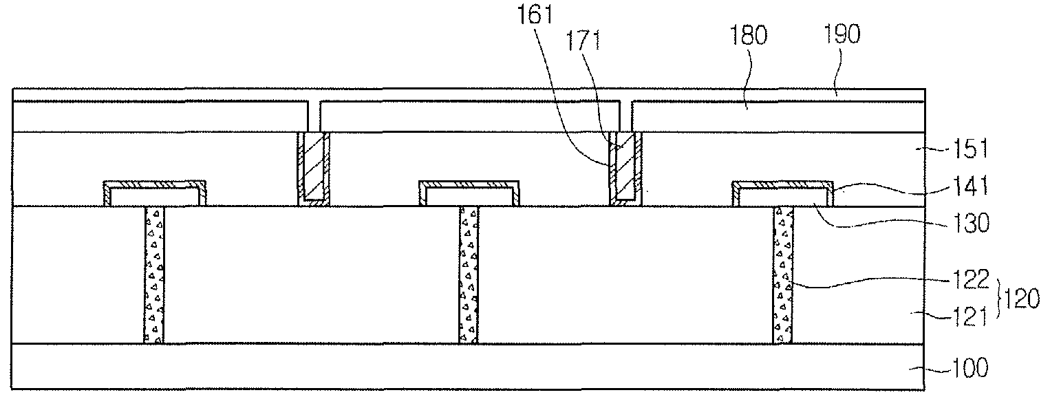
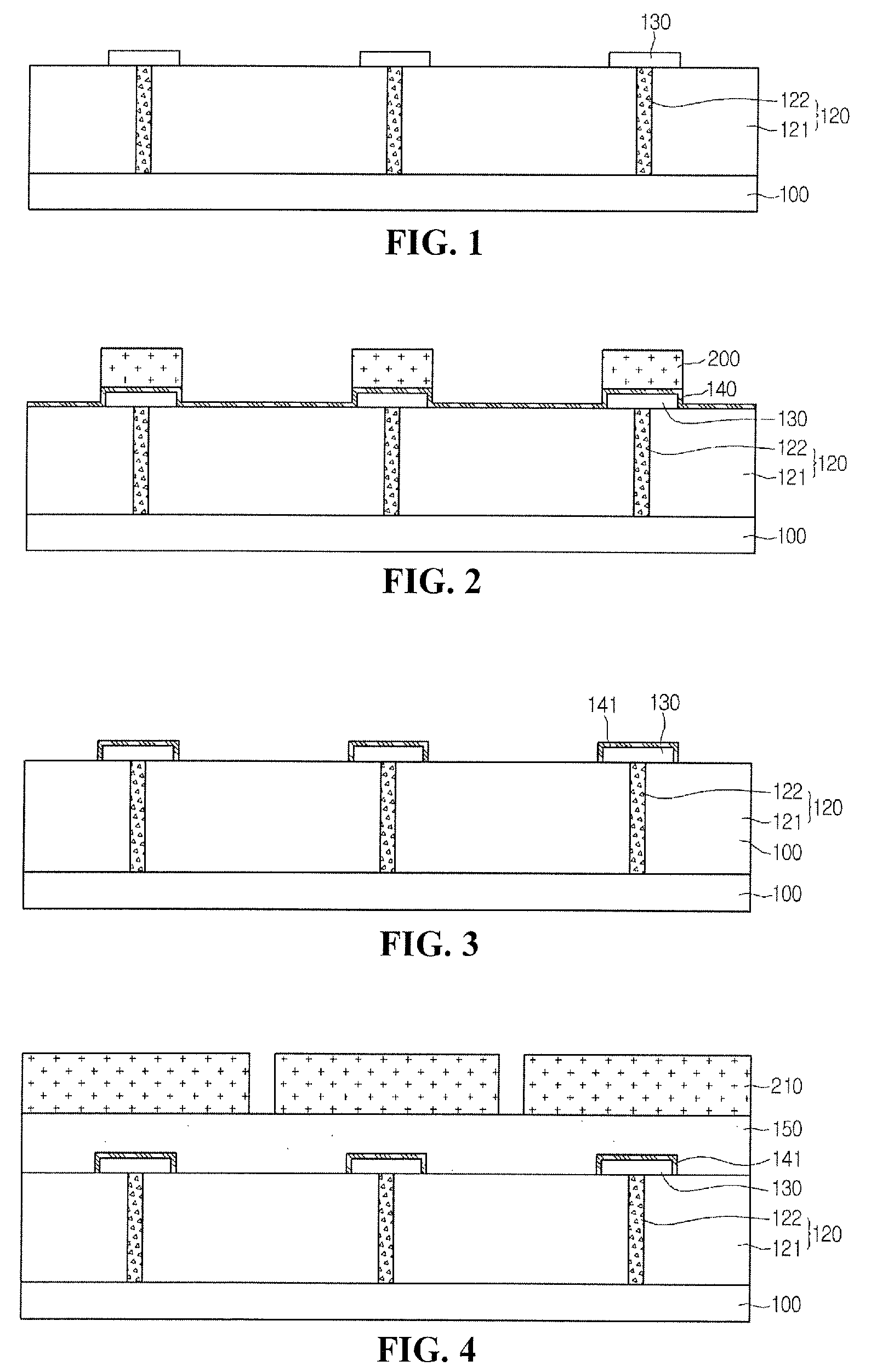
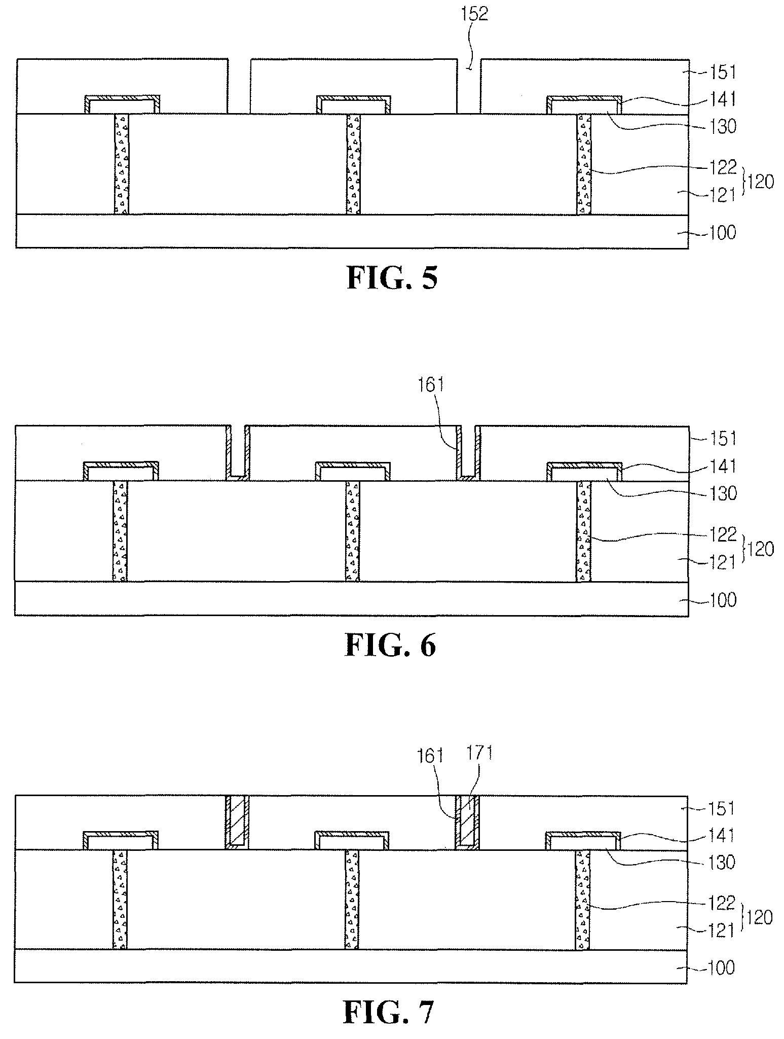
[0018]Referring to FIG. 8, the image sensor according to an embodiment of the present invention includes a semiconductor substrate 100 having a circuit region formed therein and a metal wiring layer 120, which includes a plurality of metal wirings 122 and an interlayer dielectric layer 121. Lower electrodes 130 may be formed on the metal wirings 122, with first conductive layers 141 formed to s...


PUM


Abstract

An image sensor and a method for manufacturing the same are provided. A photodiode region and transistor region are vertically-integrated to improve the fill factor and resolution of the image sensor. Unit pixels can be isolated by a metal isolation layer arranged between adjacent photodiode areas.

Description

CROSS-REFERENCE TO RELATED APPLICATION[0001]The present application claims the benefit under 35 U.S.C. §119 of Korean Patent Application No. 10-2007-0037357, filed Apr. 17, 2007, which is hereby incorporated by reference in its entirety.BACKGROUND[0002]In general, an image sensor is a semiconductor device for converting optical images into electrical signals, and is mainly classified as a charge coupled device (CCD) or a Complementary Metal Oxide Silicon (CMOS) image sensor.[0003]A CMOS image sensor sequentially detects electrical signals of pixels in a switching scheme by forming photodiodes and MOS transistors in unit pixels.[0004]A CMOS image sensor is simpler in a driving scheme than compared to a CCD image sensor. It is also capable of implementing a variety of scanning schemes and integrates signal processing in a single chip so that miniaturizing a product is possible. A CMOS image sensor uses CMOS technology so that manufacturing costs and power consumption are low.[0005]A C...

Claims


Application Information

Patent Timeline
Patent Type & Authority Patents(United States)
IPC IPC(8): H01L29/04H01L27/146H04N5/335H04N5/369H04N5/374H04N5/3745
CPCH01L27/1463H01L27/14643H01L27/14634H01L27/1469H01L27/146
Inventor KIM, TAE GYU
Owner DONGBU HITEK CO LTD
Why Eureka
Try Eureka