
Photomask, photomask fabrication method, and semiconductor device fabrication method

a fabrication method and semiconductor technology, applied in the field of photomasks, can solve the problems of increasing the possibility of transfer of circuit patterns on the wafer, and abnormalities tend to occur in circuit patterns formed on the wafer

Inactive Publication Date: 2010-09-28
FUJITSU SEMICON LTD
View PDF7 Cites 0 Cited by
  • Summary
  • Abstract
  • Description
  • Claims
  • Application Information

AI Technical Summary

Benefits of technology

The solution effectively prevents non-circuit patterns from being transferred onto the wafer, reducing flare-induced abnormalities and enhancing the reliability of circuit pattern formation by strategically placing the phase shift layer in non-circuit patterns outside the chip region.

Problems solved by technology

Accordingly, if the influence of a flare is added, an abnormality tends to occur in circuit patterns formed on the wafer.
However, locating these patterns close to the chip region increases the possibility that they are transferred onto the wafer by the influence of a flare.

Method used


Image

  • Photomask, photomask fabrication method, and semiconductor device fabrication method
  • Photomask, photomask fabrication method, and semiconductor device fabrication method
  • Photomask, photomask fabrication method, and semiconductor device fabrication method

Examples


Embodiment Construction

[0040]Embodiments of the present invention will now be described in detail with reference to the drawings.

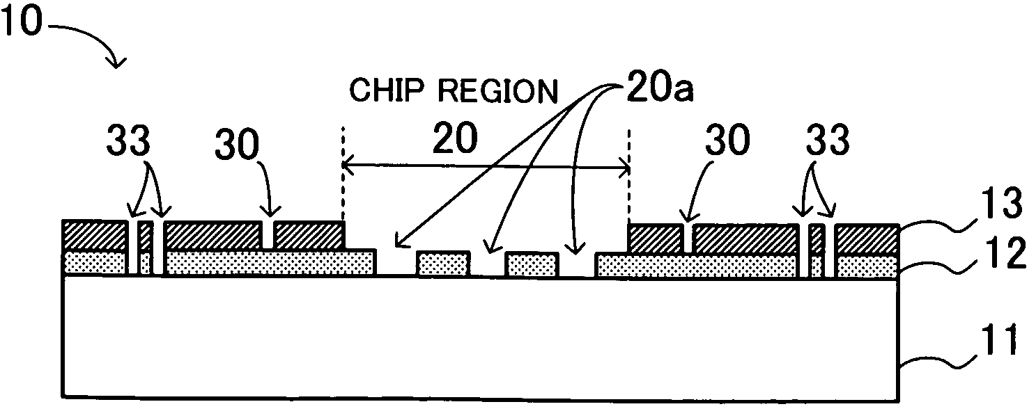
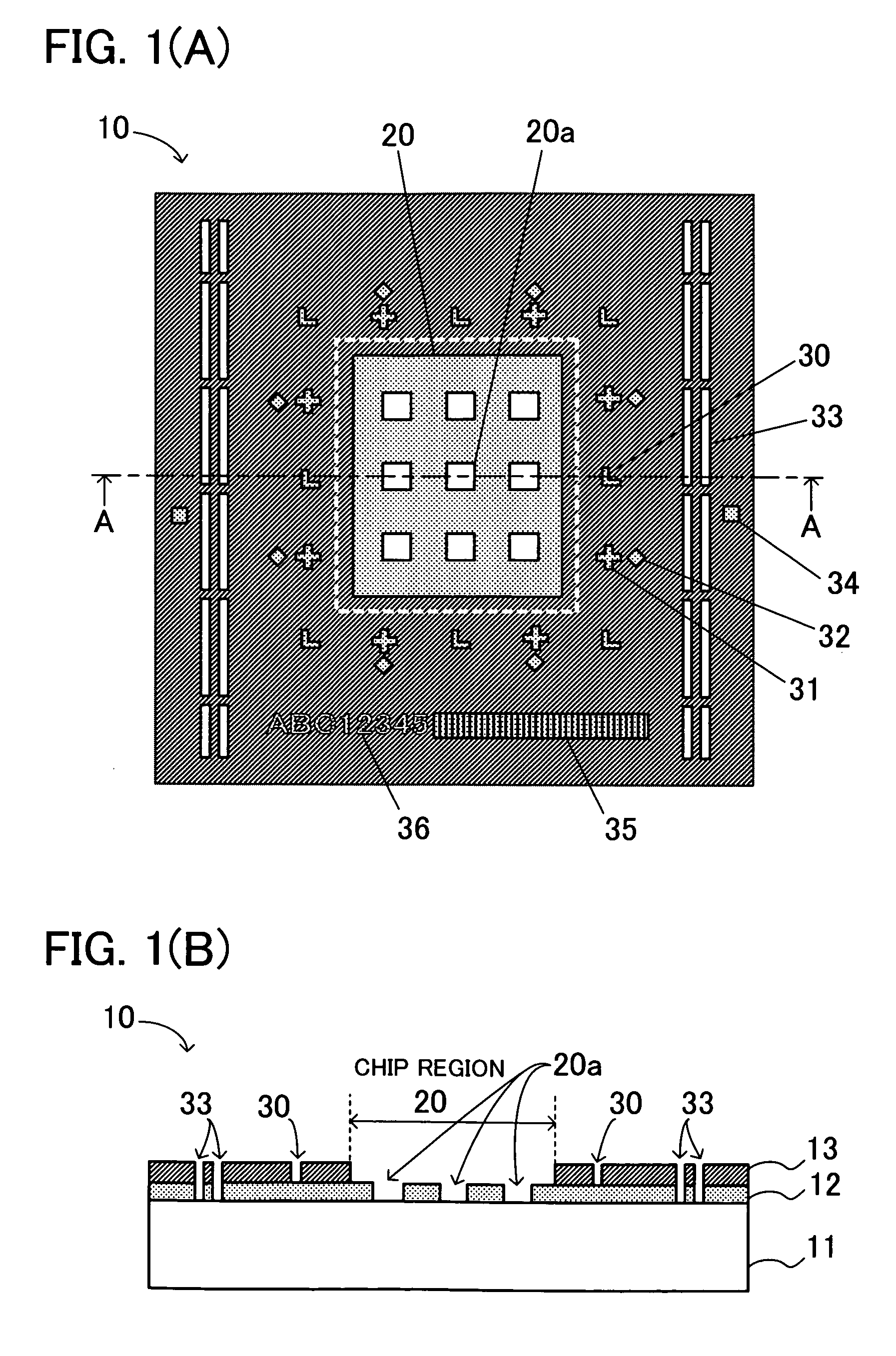
[0041]FIGS. 1(A) and 1(B) show the structure of a phase shift mask according to an embodiment of the present invention. FIG. 1(A) is a top view of the phase shift mask. FIG. 1(B) is a sectional view taken along the line A-A of FIG. 1(A).

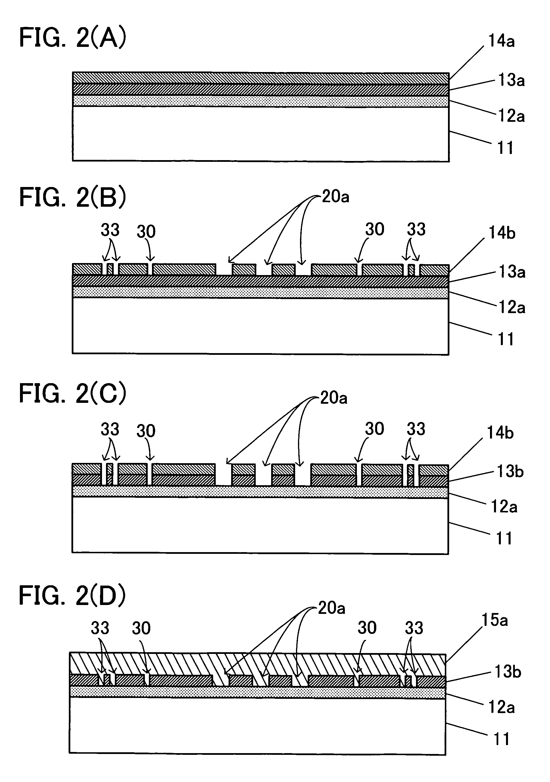
[0042]A phase shift mask 10 according to an embodiment of the present invention includes a phase shift layer 12 and a light shielding layer 13 formed in order on a transparent substrate 11. By making openings of desired shapes, patterns are formed on the phase shift mask 10.

[0043]The transparent substrate 11 is, for example, a synthetic silica substrate. Each of the phase shift layer 12 and the light shielding layer 13 can be etched selectively. For example, the phase shift layer 12 is made of MoSiON and the light shielding layer 13 is made up of a chromium film and a chromium oxide film. If the transmittance of the transparent substrate 11 is 10...


PUM

PropertyMeasurementUnit
distanceaaaaaaaaaa
transparentaaaaaaaaaa

Abstract

A photomask capable of preventing a pattern outside a chip region from being transferred onto a wafer. A non-circuit pattern (a monitor pattern for measuring the accuracy of the position of a mask pattern, for example) formed by making openings in which a phase shift layer is exposed only in a light shielding layer is located around the chip region where the light shielding layer is removed and where the phase shift layer in which openings corresponding to circuit patterns are made is exposed. This prevents the non-circuit pattern from being transferred onto the wafer by the influence of a flare.

Description

CROSS-REFERENCE TO RELATED APPLICATIONS[0001]This application is based upon and claims the benefits of priority from the prior Japanese Patent Application No. 2005-031676, filed on Feb. 8, 2005, the entire contents of which are incorporated herein by reference.BACKGROUND OF THE INVENTION[0002](1) Field of the Invention[0003]This invention relates to a photomask, a photomask fabrication method, and a semiconductor device fabrication method and, more particularly, to a photomask having the function of shifting the phase of exposure light, a method for fabricating such a photomask, and a method for fabricating a semiconductor device by the use of such a photomask.[0004](2) Description of the Related Art[0005]In recent years the formation of very fine patterns has been needed for manufacturing large-scale integrated circuits (LSIs). Accordingly, photomasks (phase shift masks) having the function of heightening contrast by shifting the phase of exposure light are used in exposure process...

Claims


Application Information

Patent Timeline
Patent Type & Authority Patents(United States)
IPC IPC(8): G03F1/00G03F1/32G03F1/68H01L21/027
CPCG03F1/14G03F1/44G03F1/26G03F1/70
Inventor ISHIWATA, NAOYUKI
Owner FUJITSU SEMICON LTD
Learn More