Semiconductor memory device and method for fabricating same
a memory device and semiconductor technology, applied in semiconductor devices, capacitors, electrical devices, etc., can solve the problems of reducing the amount of storable memory charge and difficulty in maintaining the amount of memory charge required for memory operation, and achieve the effect of improving patterning refining and small shrinkage ra
- Summary
- Abstract
- Description
- Claims
- Application Information
AI Technical Summary
Benefits of technology
Problems solved by technology
Method used
Image

Examples
first embodiment
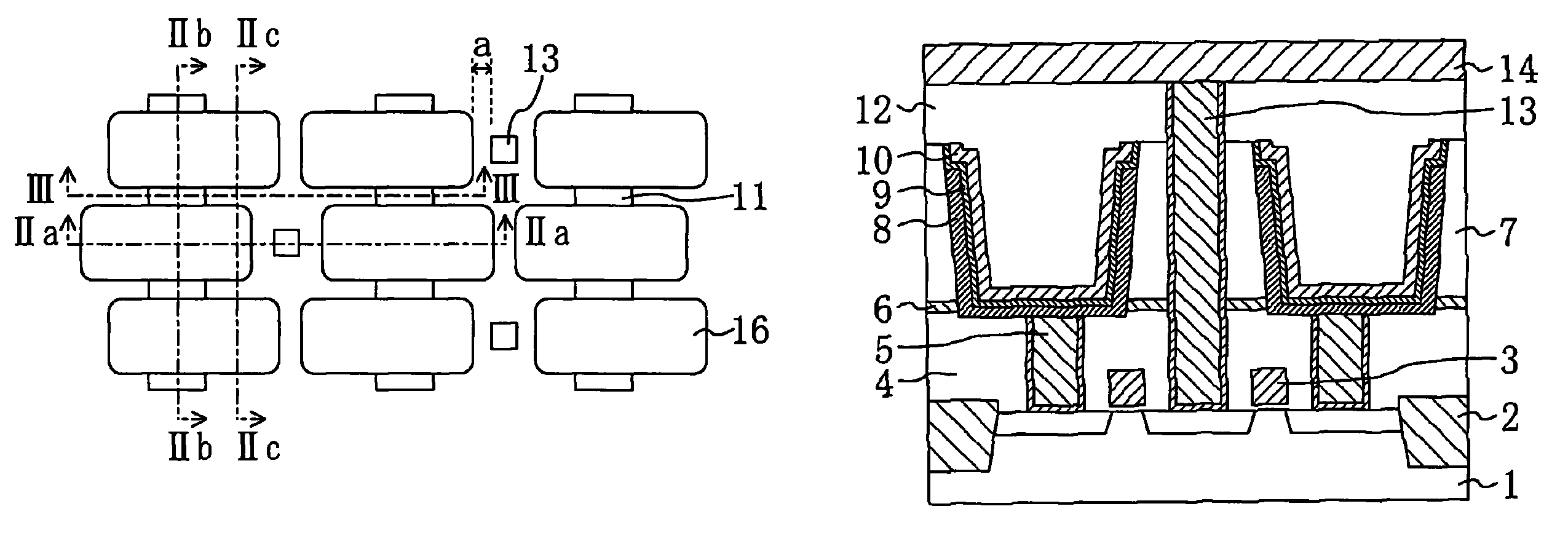
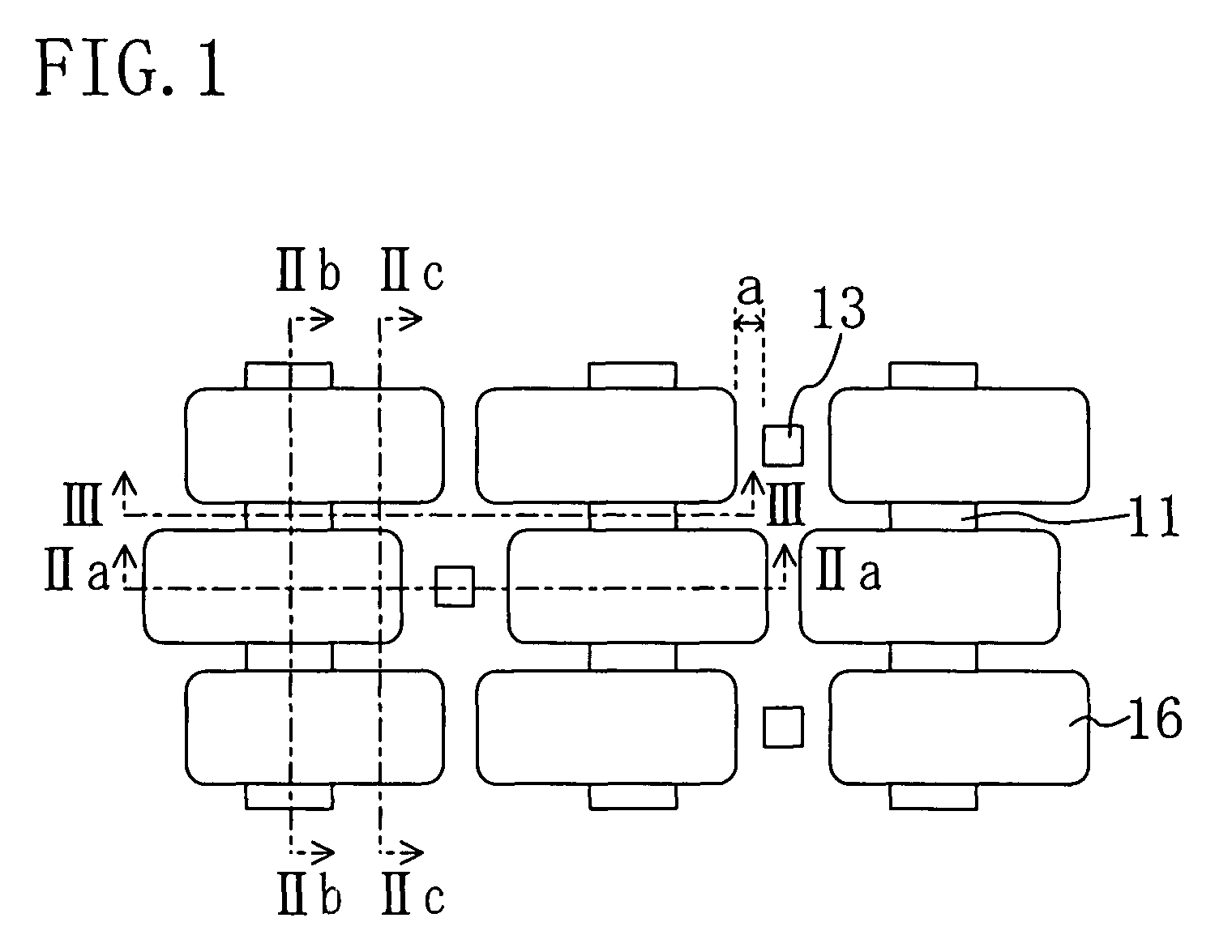
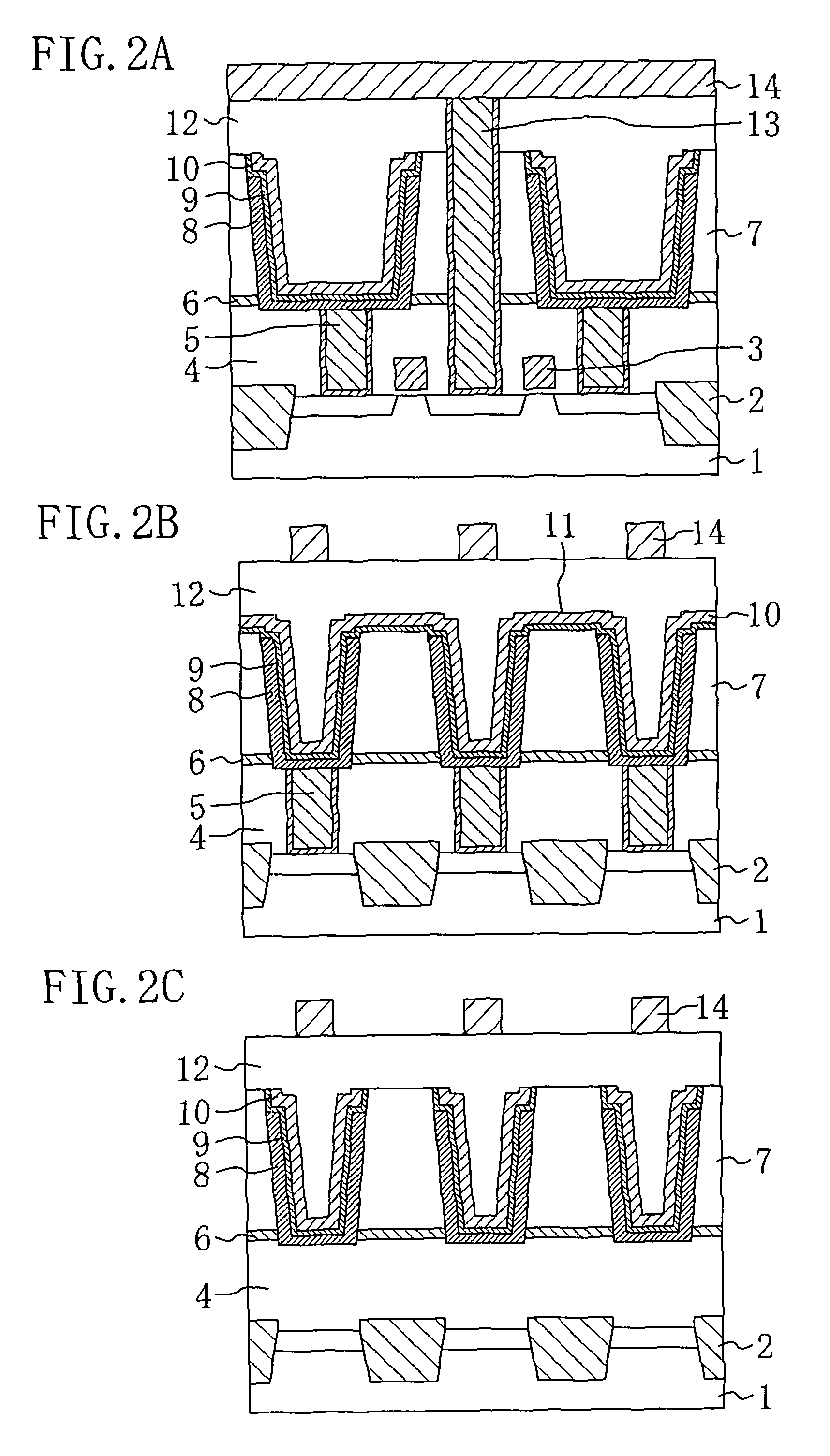
[0040]FIG. 1 is a plan view of a semiconductor memory device of the CUB structure according to the first embodiment. FIG. 2A is a cross sectional view of the device taken along the line IIa-IIa shown in FIG. 1, FIG. 2B is a cross sectional view of the device taken along the line IIb-IIb shown in FIG. 1, FIG. 2C is a cross sectional view of the device taken along the line IIc-IIc shown in FIG. 1, and FIG. 3 is a cross sectional view of the device taken along the line III-III shown in FIG. 1.
[0041]As shown in FIGS. 1 and 2A, the semiconductor memory device according to this embodiment has: a capacitor opening portion 16 provided in a first interlayer insulating film 7 formed on a semiconductor substrate 1; and a capacitance element composed of a lower electrode 8, a capacitance insulating film 9, and an upper electrode 10, which are formed over the bottom and sides of the capacitor opening portion. Through the first interlayer insulating film 7 is formed a bit-line contact plug 13. At...
second embodiment
[0061]FIGS. 10A through 10C are views of a semiconductor memory device of the CUB structure according a second embodiment, showing the structure of the device. FIG. 10A is a plan view of the device, FIG. 10B is a cross sectional view of the device taken along the line Xb-Xb shown in FIG. 10A., and FIG. 10C is a cross sectional view of the device taken along the line Xc-Xc shown in FIG. 10A.
[0062]A method for fabricating the semiconductor memory device according to this embodiment will be described in conjunction with cross sectional views of the device shown in FIGS. 10A through 13C. In the figures, the region A denotes a cross section of the device taken along the line Xb-Xb in FIG. 10A, and the region B denotes a cross section of the device taken along the line Xc-Xc in FIG. 10A. Steps that the first and second embodiments have in common will not be described in detail.
[0063]First, referring to FIG. 11A, an element isolating oxide film 2 made of a silicon oxide film is formed on a...
third embodiment
[0071]FIGS. 14A and 14B are cross sectional views of a semiconductor memory device according to a third embodiment of the present invention, showing the process of fabricating the semiconductor memory device. The layout of the memory cells of this embodiment is the same as the layout shown in FIG. 1. In the figures, the region A denotes a cross section of the device taken along the line IIa-IIa in FIG. 1, and the region B denotes a cross section of the device taken along the line IIb-IIb in FIG. 1.
[0072]First, the upper electrode 8 is formed in the capacitor opening portion 16 through similar steps to those in the first embodiment as shown in FIG. 4A through 5B.
[0073]Next, referring to FIG. 14A, over the first interlayer insulating film 7 including the inside of the capacitor opening portion 16, an insulating film 9 for use in forming a capacitance insulating film and a conductive film 10 for use in forming an upper electrode are accumulated, followed by formation of a line-form res...
PUM
 Abstract
Description
Claims
Application Information
 - R&D
- Intellectual Property
- Life Sciences
- Materials
- Tech Scout
- Unparalleled Data Quality
- Higher Quality Content
- 60% Fewer Hallucinations
Browse by: Latest US Patents, China's latest patents, Technical Efficacy Thesaurus, Application Domain, Technology Topic, Popular Technical Reports.
© 2025 PatSnap. All rights reserved.Legal|Privacy policy|Modern Slavery Act Transparency Statement|Sitemap|About US| Contact US: help@patsnap.com