
Memory device using abrupt metal-insulator transition and method of operating the same

a technology of metal-insulator transition and memory device, which is applied in the direction of semiconductor devices, digital storage, instruments, etc., can solve the problems of resistance change memory device undergoing a structural phase change of resistance change material, resistance change memory device may lose memory characteristics after long use, and achieve high-speed switching operation

Inactive Publication Date: 2010-09-07
ELECTRONICS & TELECOMM RES INST
View PDF13 Cites 2 Cited by
  • Summary
  • Abstract
  • Description
  • Claims
  • Application Information

AI Technical Summary

Benefits of technology

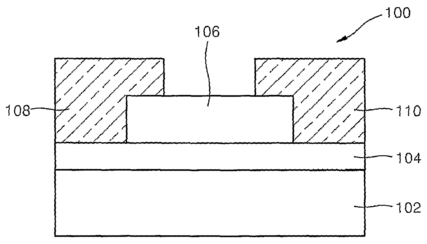
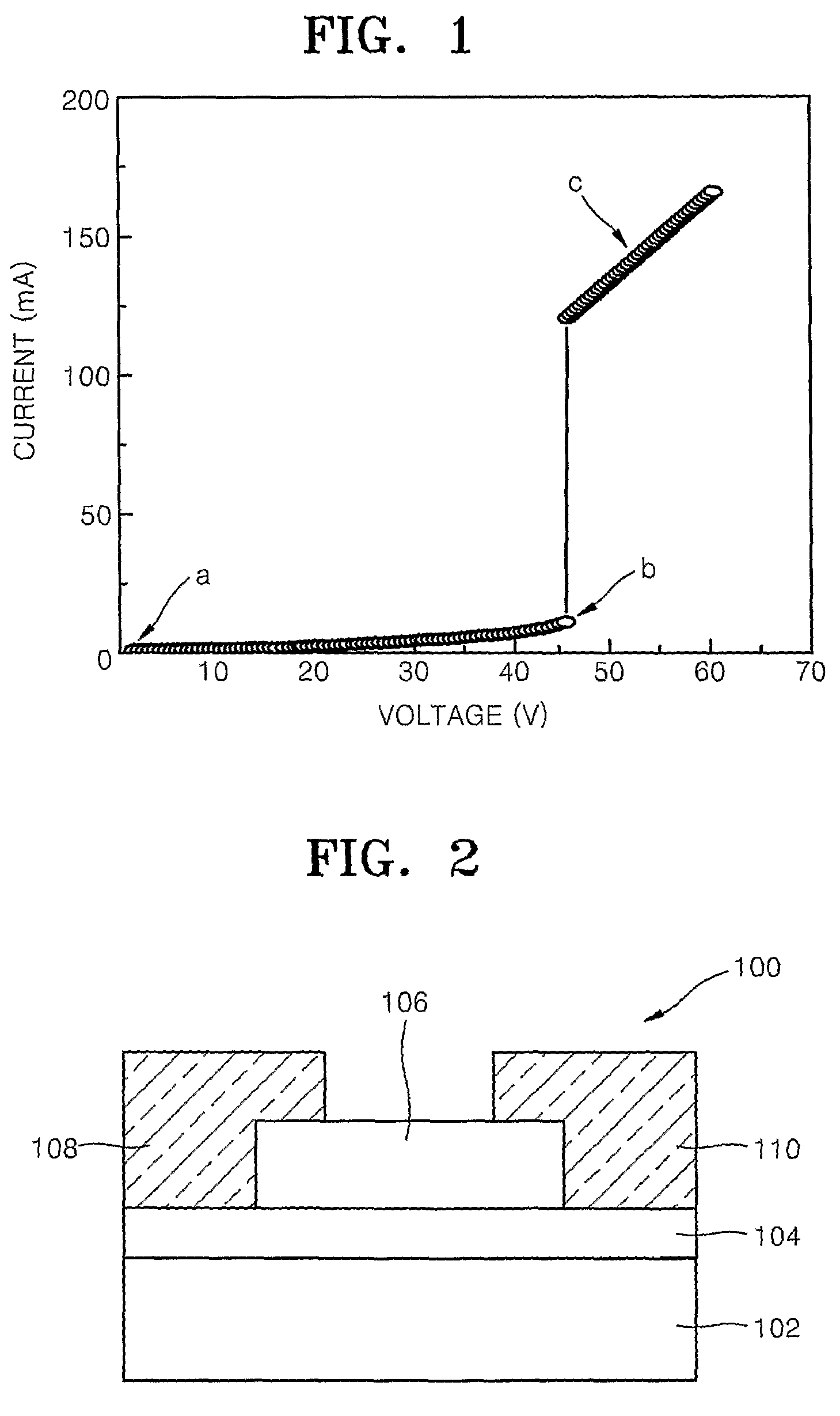
The present invention provides a memory device that has no structural phase change, maintains a uniform thin film, and can perform high-speed switching operations. The device includes an abrupt MIT material layer that undergoes an abrupt MIT by an energy change between electrons and a plurality of electrodes that are melted by heat to form a conductive path on the abrupt MIT material layer. The plurality of electrodes may be monocrystalline or polycrystalline and may be disposed at a predetermined distance from each other to ensure sufficient formation of the conductive path. The method of operating the memory device involves forming the abrupt MIT material layer, bringing the electrodes into contact with the abrupt MIT material layer, applying a first voltage to the electrodes to melt them and create the conductive path, and maintaining the abrupt MIT material layer with a metallic phase. The memory device may maintain an on-state when the first voltage is applied and maintain an off-state when the second voltage is applied.

Problems solved by technology

This phase change memory device requires a high melting temperature of a phase change material and a large amount of time for crystallization, and is thus unreliable in a repetitive switching operation.
However, the resistance change memory device undergoes a structural phase change of the resistance change material.
Also, when the dendrite conductor is not created or is low in concentration, the resistance change memory device cannot meet memory characteristics.
Furthermore, since the resistance change memory device generates heat in the high-resistance state, the resistance change memory device may lose memory characteristics after long usage.
In summary, since the phase change memory device and the resistance change memory device undergo a structural phase change, the phase change memory device and the resistance change memory device are unsuitable as a high-speed switching device.

Method used


Image

  • Memory device using abrupt metal-insulator transition and method of operating the same
  • Memory device using abrupt metal-insulator transition and method of operating the same
  • Memory device using abrupt metal-insulator transition and method of operating the same

Examples


Embodiment Construction

[0028]The present invention will now be described more fully with reference to the accompanying drawings, in which exemplary embodiments of the invention are shown. The invention may, however, be embodied in many different forms and should not be construed as being limited to the embodiments set forth herein; rather, these embodiments are provided so that this disclosure will be thorough and complete, and will fully convey the concept of the invention to those skilled in the art. Like reference numerals in the drawings denote like elements, and thus their description will be omitted.

[0029]The embodiments of the present invention propose memory devices that use an abrupt MIT material layer and thus undergo no structural phase change. Since the memory devices undergo no structural phase change, a high-speed switching operation is possible and the probability of the occurrence of defects can decrease greatly. Accordingly, it is possible to manufacture a high-quality memory device. The ...


PUM


Abstract

Provided are a memory device that undergoes no structural phase change, maintains a uniform thin film, and can perform a high-speed switching operation, and a method of operating the same. The memory device includes a substrate, an abrupt MIT material layer, and a plurality of electrodes. The abrupt MIT material layer is disposed on the substrate and undergoes an abrupt metal-insulator transition by an energy change between electrons. The plurality of electrodes are brought into contact with the abrupt MIT material layer and are melted by heat to form a conductive path on the abrupt MIT material layer.

Description

CROSS-REFERENCE TO RELATED PATENT APPLICATION[0001]This application claims the benefit of Korean Patent Application No. 10-2005-0058654, filed on Jun. 30, 2005, and No. 10-2006-0015634, filed on Feb. 17, 2006, in the Korean Intellectual Property Office, the disclosures of which are incorporated herein in its entirety by reference.BACKGROUND OF THE INVENTION[0002]1. Field of the Invention[0003]The present invention relates to a memory device and a method of operating the same, and more particularly, to a memory device using an abrupt metal-insulator transition (MIT) and a method of operating the same.[0004]2. Description of the Related Art[0005]An example of a memory device is a phase change memory device that uses a structural phase change between a crystalline phase and an amorphous phase. This phase change memory device requires a high melting temperature of a phase change material and a large amount of time for crystallization, and is thus unreliable in a repetitive switching ope...

Claims


Application Information

Patent Timeline
Patent Type & Authority Patents(United States)
IPC IPC(8): H01L45/00G11C11/00H10K99/00
CPCB82Y10/00G11C13/0007G11C13/0014H01L27/10H01L29/8615H01L45/04H01L45/1226H01L45/1233H01L45/146H01L45/148G11C2213/32G11C2213/51H01L49/003H10N70/823H10N70/20H10N70/884H10N70/826H10N70/8833H10B99/10H10N99/03
Inventor KIM, HYUN-TAKKIM, BONG-JUNKANG, KWANG-YONGYUN, SUN-JINLEE, YONG-WOOKCHAE, BYUNG-GYU
Owner ELECTRONICS & TELECOMM RES INST
Learn More