
Scanning electron microscope with length measurement function and dimension length measurement method

a scanning electron microscope and function technology, applied in the field of scanning electron microscopes with length measurement functions and sample dimension measurement methods, can solve the problems of large dimension error, unstable detection amount of electrons, and large dimension error, so as to improve the length measurement accuracy and reduce the variation of measured values

Active Publication Date: 2010-09-07
ADVANTEST CORP
View PDF12 Cites 3 Cited by
  • Summary
  • Abstract
  • Description
  • Claims
  • Application Information

AI Technical Summary

Benefits of technology

This approach enables high-accuracy length measurements by maintaining consistent electron beam irradiation, reducing measurement errors attributed to pattern shape and material variations, and optimizing measurement time through raster or vector scans.

Problems solved by technology

Consequently, a problem occurs in which a detected amount of electrons becomes unstable.
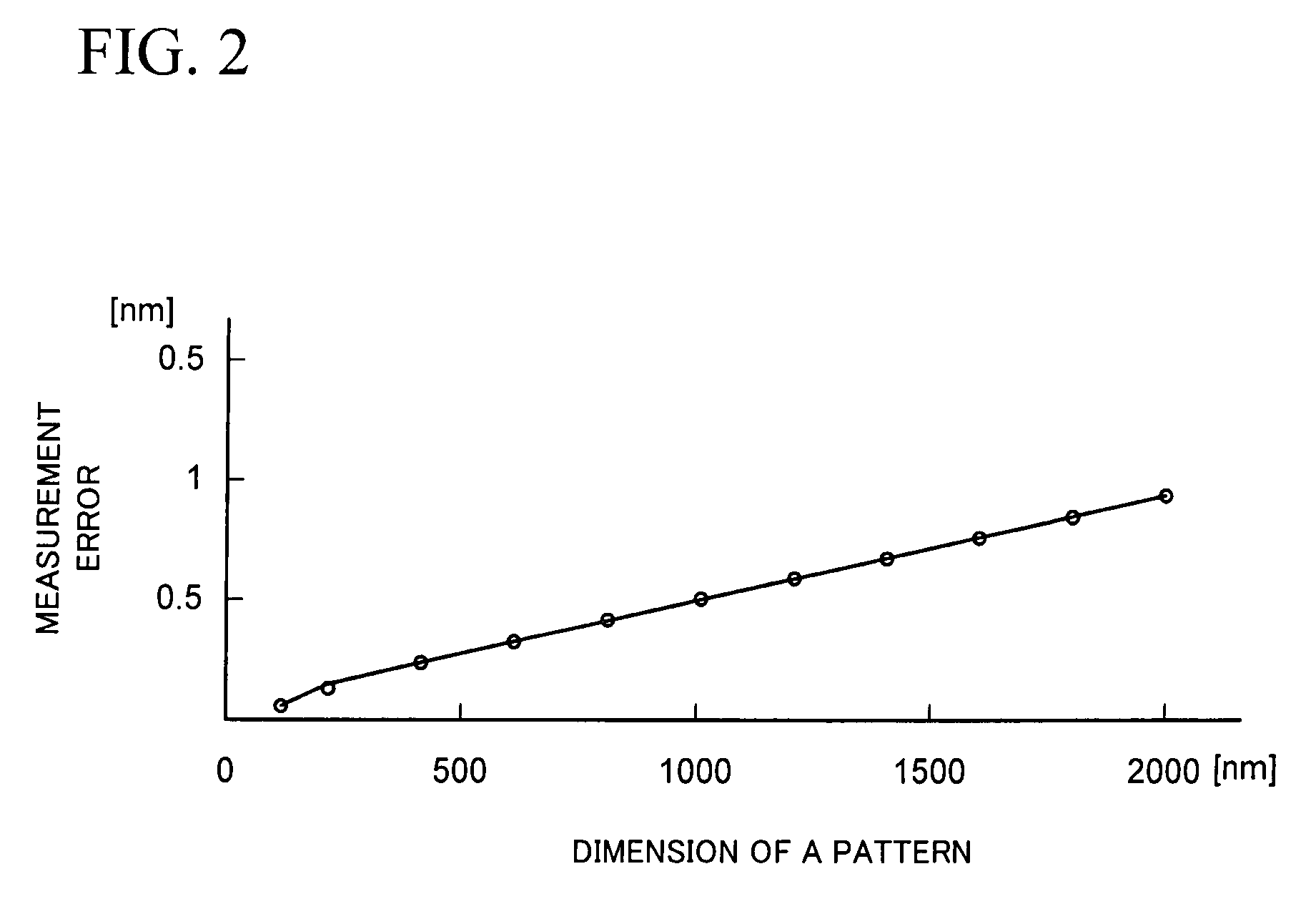
When the line width of the pattern of a measurement target is increased, a phenomenon occurs in which dimension error becomes large.
Because of the influence of this charge-up, a primary beam is deflected so that a length measurement magnification is changed, thus causing a dimension measurement error.

Method used


Image

  • Scanning electron microscope with length measurement function and dimension length measurement method
  • Scanning electron microscope with length measurement function and dimension length measurement method
  • Scanning electron microscope with length measurement function and dimension length measurement method

Examples


Embodiment Construction

[0030]Embodiments of the present invention are described below with reference to the accompanying drawings.

[0031]First, a configuration of a scanning electron microscope with a length measurement function is described. Then, a concept of making an accurate length measurement of a pattern is described. Next, a sample dimension measurement method, using the scanning electron microscope with the length measurement function, is described.

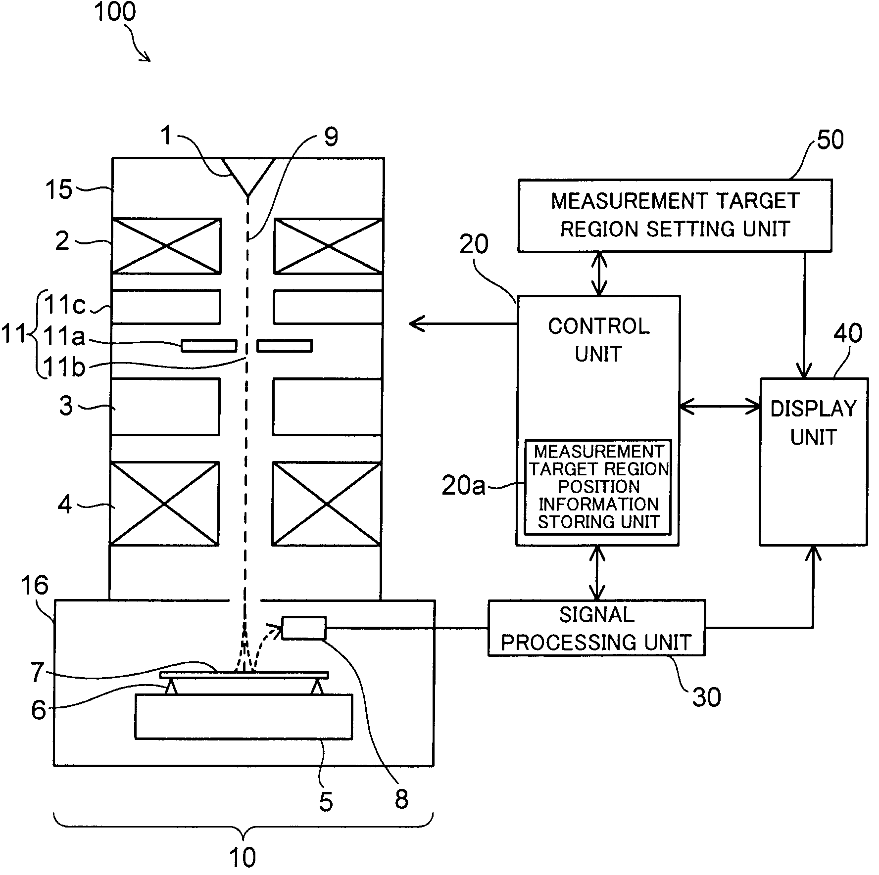
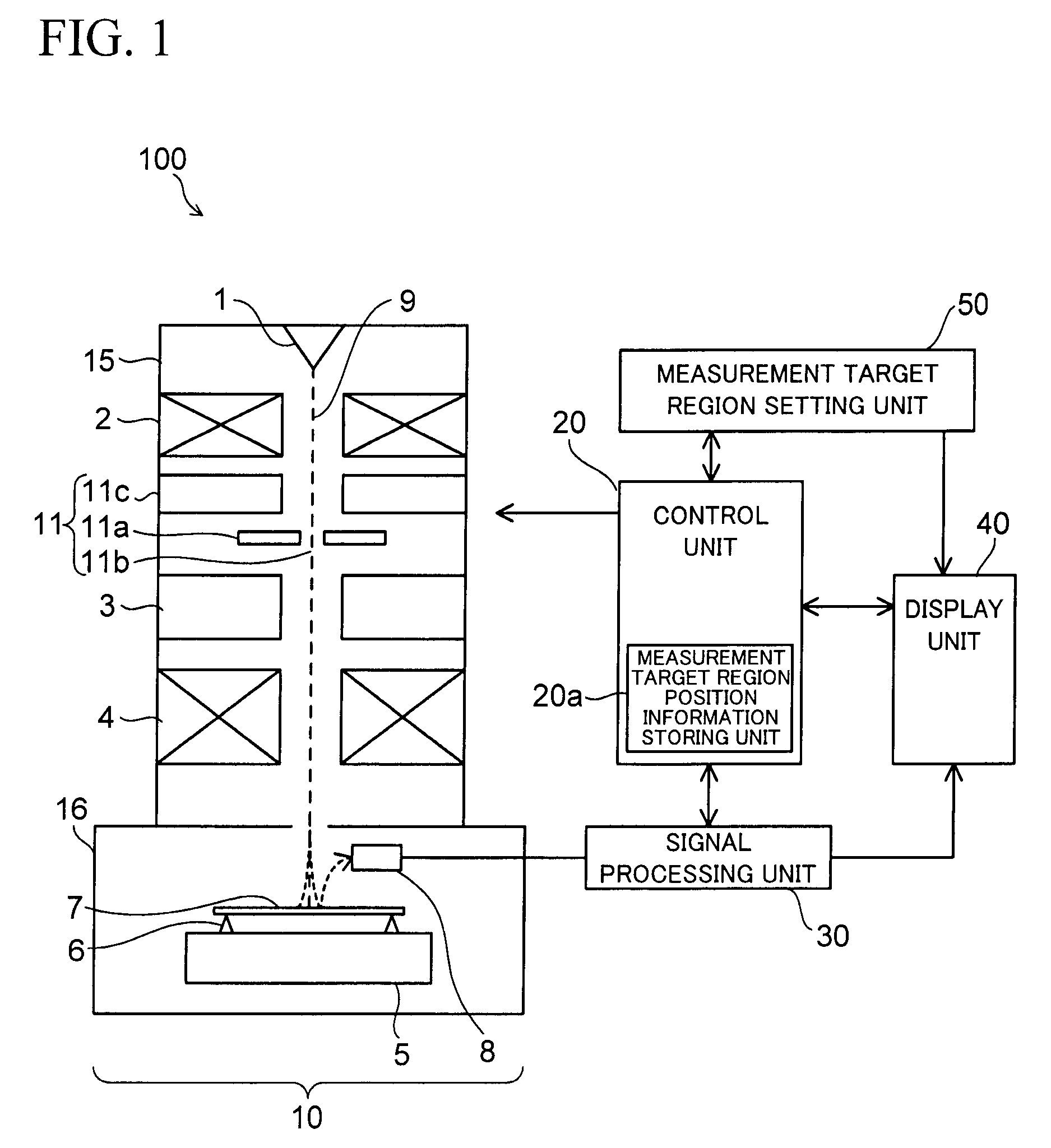
[0032]FIG. 1 is a configuration diagram of a scanning electron microscope of a present embodiment.

[0033]Such a scanning electron microscope 100 is roughly divided into an electron scanning unit 10, a signal processing unit 30, a display unit 40, a measurement target region setting unit 50, and a control unit 20 which controls the electron scanning unit 10, the signal processing unit 30, the display unit 40, and the measurement target region setting unit 50. The electron scanning unit 10 includes an electron optical column unit 15 and a sample chamber 16...


PUM


Abstract

A scanning electron microscope with a length measurement function includes an electron gun for emitting an electron beam, a measurement target region setting unit for setting a measurement region for a pattern formed on a sample, a storing unit for storing the designated measurement region, a beam blanker unit for controlling an irradiation of the electron beam depending on the measurement region, and a control unit for extracting the designated measurement region from the storing unit, interrupting the electron beam with the beam blanker unit in a region other than the measurement region, irradiating the electron beam onto the sample in the measurement region, capturing an image of the measurement region, and measuring the pattern. The measurement region may be a pair of regions having the same areas as each other.

Description

[0001]This application claims the benefit of U.S. Provisional Patent Application Ser. No. 60 / 906,619 filed Mar. 13, 2007 and U.S. Provisional Patent Application Ser. No. 60 / 922,513 filed Apr. 9, 2007, all of which are hereby incorporated by reference.BACKGROUND OF THE INVENTION[0002]1. Field of the Invention[0003]The present invention relates to a scanning electron microscope with a length measurement function, and a sample dimension measurement method to observe and measure a sample by irradiating an electron beam onto the sample.[0004]2. Description of the Prior Art[0005]In the processes of manufacturing semiconductor devices, observation of a sample, measurement of a line width of a pattern and the like are performed by using an electron beam device such as an electron microscope. In observation and measurement of a sample performed by the electron beam device, a scanning operation is performed in the following manner: while an electron beam is irradiated onto a portion of the sa...

Claims


Application Information

Patent Timeline
Patent Type & Authority Patents(United States)
IPC IPC(8): H01J37/26
CPCG01B15/00H01J37/045H01J37/265H01J37/28H01J2237/004H01J2237/24585H01J37/06
Inventor NAKAMURA, TAKAYUKIIWAI, TOSHIMICHISHIDA, SOICHIHIROYAMA, MITSUO
Owner ADVANTEST CORP
Learn More