Amplifier

a technology of amplifiers and amplifiers, applied in the field of amplifiers, can solve the problems of linearity degradation, increased power consumption, and reduced power added efficiency, and achieve the effect of high power added efficiency

Active Publication Date: 2010-08-03
NEC CORP
View PDF23 Cites 12 Cited by
  • Summary
  • Abstract
  • Description
  • Claims
  • Application Information

AI Technical Summary

Benefits of technology

[0064]It is a second object of the present invention to provide an approach for employing amplification stages having a gain expansion characteristic by biasing to a state close to B-class with high power added efficiency at low output at all stages of a multi-stage amplifier.
[0067]According to the present invention, distortions at respective stages can cancel out each other in a multi-stage amplifier. Also, an amplification stage biased in a state close to B-class, which exhibits high power added efficiency at low output, can be used at all stages of the multi-stage amplifier.

Problems solved by technology

In other words, the saturation characteristic is degraded to cause a reduction in power added efficiency and a degradation in linearity.
Also, when the collector bias current is set equivalent to a collector current when a base bias is applied by a regulated voltage source and when the input power is large, a collector current flows even when no RF signal is supplied and the input power is small, thus giving rise to a problem of increased power consumption and the like.
However, when voltage amplitude V2 at B1 point increases, as the input power increases, and exceeds the potential difference between bias voltage VB1 applied to the aforementioned B1 point and ON voltage Vth of the base-emitter diode, as indicated by V2 in FIG. 5, transistor Tr1 enters a non-linear operation state, and cannot maintain the operation point as the A-class, so that the power gain gradually decreases.
However, as the input power becomes higher to cause an increase in the bias current flowing into diode D1, the voltage becomes lower due to a voltage drop caused by resistor R1, and even the potential at B2 point in FIG. 2 becomes lower, so that the circuit can no longer operate as a regulated voltage source.
There is therefore a first problem that the current flowing through resistor R2 must be increased to such a degree that the current flowing into diode D1 can be neglected.
Though reduced, however, the second conventional amplifier is similar to the first conventional amplifier in that it suffers from the first problem that the current flowing through resistor R2 must be increased to such a degree that the current flowing into the base of transistor Tr2 can be neglected.
However, in the first and second bias circuits, which generate this voltage through resistance division using resistors R1, R2, a second problem arises in that they are strongly affected by fluctuations in voltage between the base and emitter due to the temperature, variations attributable to the manufacturing, and the like.
However, the bias circuit of the second conventional amplifier illustrated in FIG. 4 has the first problem that the current flowing through resistor R2 must be increased to such a degree that the current flowing into the base of transistor Tr2 can be neglected, whereas in the bias circuit of the third conventional amplifier in FIG. 6, since the value of Iref can be reduced if a large area ratio is selected, the value of R17 can be increased to keep fluctuations small.
The gain fluctuates when this amplifier having the gain expansion characteristic is applied with a broadband modulated signal associated with a change in power, such as a W-CDMA signal, wherein a third problem arises in that the fluctuations in the gain cause a signal distortion.
For simplicity, these conventional examples are collectively called the “fourth conventional amplifiers.” These fourth conventional amplifiers combine the gain expansion amplification stage with the gain compression amplification stage to reduce distortions, and therefore have a fourth problem of the inability to apply an amplifier that exhibits the gain expansion characteristic with good power added efficiency at low output to all amplification stages.
However, since injection amount D cannot be selected to reduce IM3 independently of the value of input amplitude A, it is necessary to optimize the injection amount by any method such as feed-back, feed-forward or the like.
As the third problem mentioned above, the first to third conventional amplifiers have a drawback in which signals are distorted due to the gain expansion when they are used as biased in a state close to B-class in order to increase the power added efficiency at low output.
Also, as the fourth problem mentioned above, the fourth conventional amplifier has a drawback of the inability to employ the amplification stage, which exhibits a good power added efficiency at low output, at all stages due to the third problem mentioned above.
Then, as the fifth problem mentioned above, the fifth conventional amplifier has a drawback that there is a requirement for adjustment of the injection amount through feed-back, feed-forward or the like in the injection of a differential frequency signal due to the dependence of an optimal injection amount on the input amplitude.

Method used


Image

  • Amplifier
  • Amplifier
  • Amplifier

Examples


first embodiment

[0171]FIG. 24 is a diagram illustrating an amplifier which inverts the phase of IM3 with respect to a basic wave according to a first embodiment of the present invention. Amplifying transistor 1 forms an emitter grounded amplifier circuit, where transistor 1 has a base, through impedance element 2, which is connected to input matching circuit 3 and to a cathode of bias supply diode 4. Bias supply diode 4 has an anode connected to reference power supply 5 which presents a sufficiently low impedance at high frequencies. Transistor 1 has a collector connected to collector power supply 7 through load 6 and to output terminal 9 through output matching circuit 8.

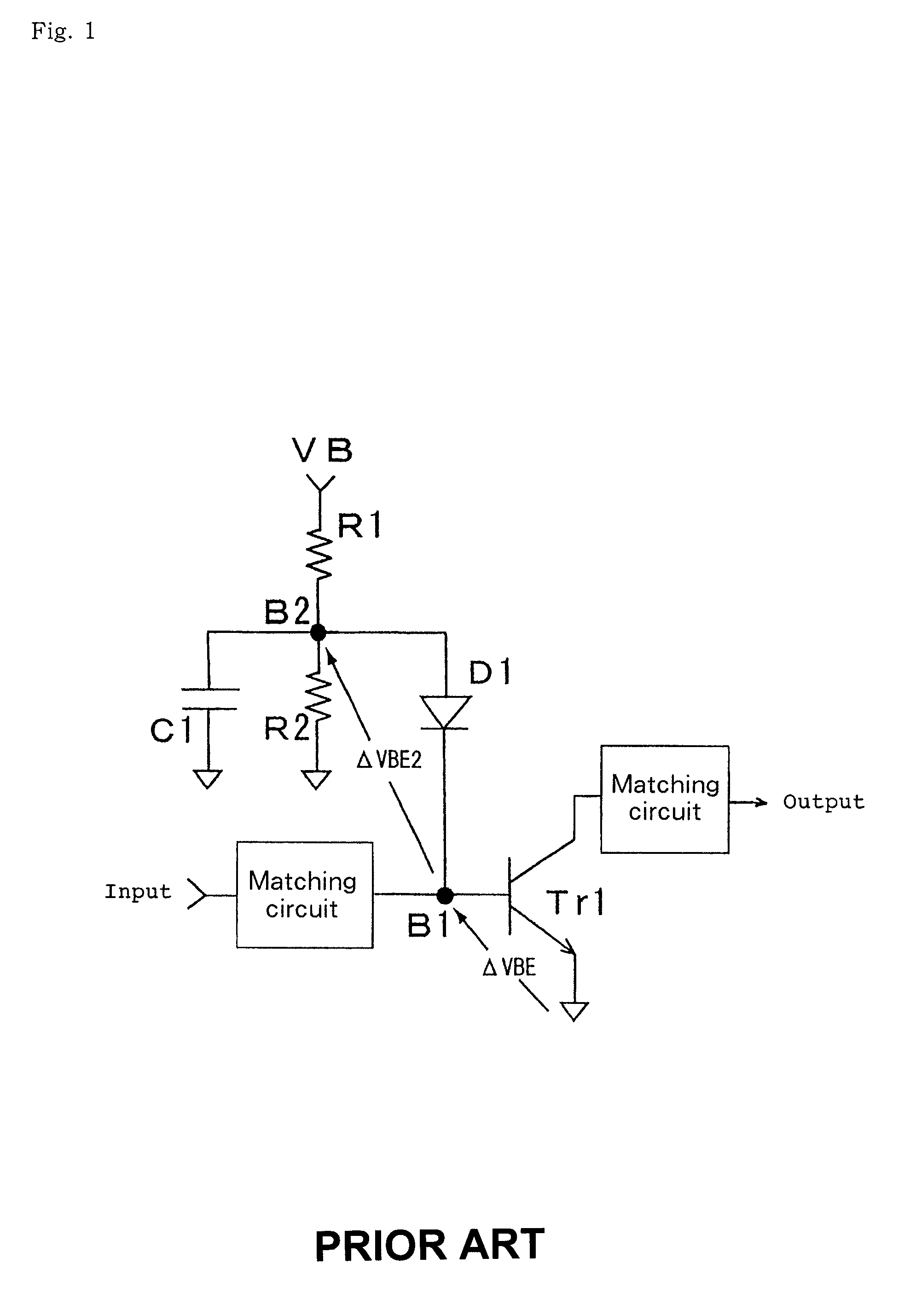
[0172]FIG. 24, which illustrates this embodiment, corresponds to FIG. 1 which illustrates the first conventional example. In comparing the first embodiment illustrated in FIG. 24 with the first conventional example of FIG. 1, bias supply diode D1 has the cathode connected directly to the base terminal of amplifying transistor Tr1 ...

second embodiment

[0173]FIG. 27 is a diagram illustrating an amplifier which inverts the phase of IM3 with respect to the basic wave according to a second embodiment of the present invention, and corresponds to FIG. 4 of the second conventional example. This embodiment uses the base-emitter of bias supply transistor 11 instead of diode 4 in the first embodiment. Therefore, the effect and operation are the same as those of the first embodiment. This embodiment alleviates the aforementioned second problem in which, when reference power supply 5 is implemented by a resistor, the resistor causes a voltage drop. In this embodiment, since the bias is also supplied to amplifying transistor 1 through impedance element 21, this impedance element 21 does not block any DC current. Since this embodiment is substantially identical to the aforementioned first embodiment in effect and operation, they will be jointly described below in this embodiment.

[0174]FIG. 25 is a diagram for describing the second embodiment o...

third embodiment

[0181]FIG. 30 is a diagram illustrating an amplifier which inverts the phase of IM3 with respect to the basic wave according to a third embodiment of the present invention. Amplifying transistor 1 forms an emitter grounded amplifier circuit, where the base of transistor 1 is biased by bias supply diode 23. Also, the same transistor 1 has a base connected to input matching circuit 3 and bias supply diode 24 through impedance element 25. Anodes of Bias supply diodes 23 and 24 have their anodes connected to reference power supply 5. Transistor 1 has a collector which is connected to collector power supply 7 through load 6 and which is also connected to output terminal 9 through output matching circuit 8.

[0182]Since this embodiment is identical in effect and operation to a fourth to a sixth embodiment, later described, they will be jointly described in the sixth embodiment.


PUM


Abstract

The present invention provides compensation for distortions in a multi-stage amplifier having a gain expansion characteristic. The present invention also provides an approach for using an amplification stage biased in a state close to B-class, which exhibits high power with added efficiency at low output, in order to have a gain expansion characteristic in all stages of a multi-stage amplifier. The amplifier of the present invention has a gain expansion characteristic which presents an increase in gain in response to an increase in input power or output power in a certain range of the input power or the output power. The amplifier is characterized in that an emitter grounded amplifier circuit comprising a first bipolar transistor has a base terminal to which an input matching circuit and a cathode of a first diode for supplying a bias voltage are connected through a first impedance element which does not block a direct current, and the first diode has an anode which is connected to a reference power supply which presents a sufficiently low impedance at high frequencies.

Description

[0001]This application claims priority from PCT Application No. PCT / JP2004 / 019526 filed Dec. 27, 2004, and from Japanese Patent Application No. 2004-000672 filed Jan. 5, 2004, which applications are incorporated herein by reference.TECHNICAL FIELD[0002]The present invention relates to an amplifier, and more particularly, to an amplifier, for use in radio communications to control output power over a wide range, which amplifies input power by a plurality of transistors connected at multiple stages to generate amplified power.BACKGROUND ART[0003]A power amplifier employing an emitter grounded bipolar transistor indispensably requires a base bias circuit which operates in a manner close to a regulated voltage source. A regulated voltage source is more suitable for a bias circuit than a regulated current source for reasons set forth below.[0004]Consider that an RF input is applied to an emitter grounded bipolar transistor which is applied with a bias at a base from a regulated voltage s...

Claims


Application Information

Patent Timeline
Patent Type & Authority Patents(United States)
IPC IPC(8): H03F1/00H03F1/02H03F1/30H03F1/32H03F3/343
CPCH03F1/0266H03F1/302H03F1/3276H03F3/343
Inventor AOKI, YUUICHI
Owner NEC CORP
Why Eureka
Try Eureka