
Light emitting device having TFT

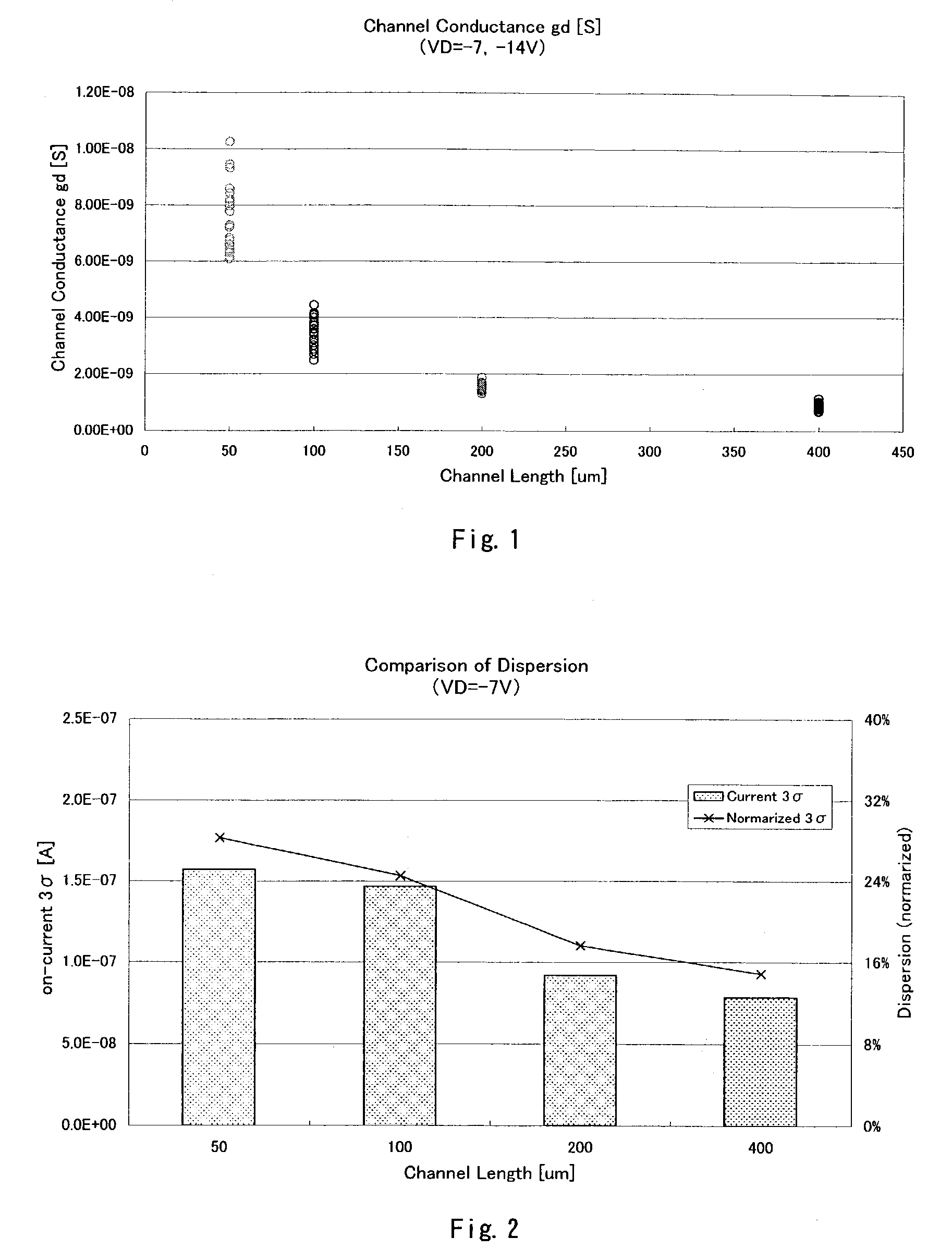
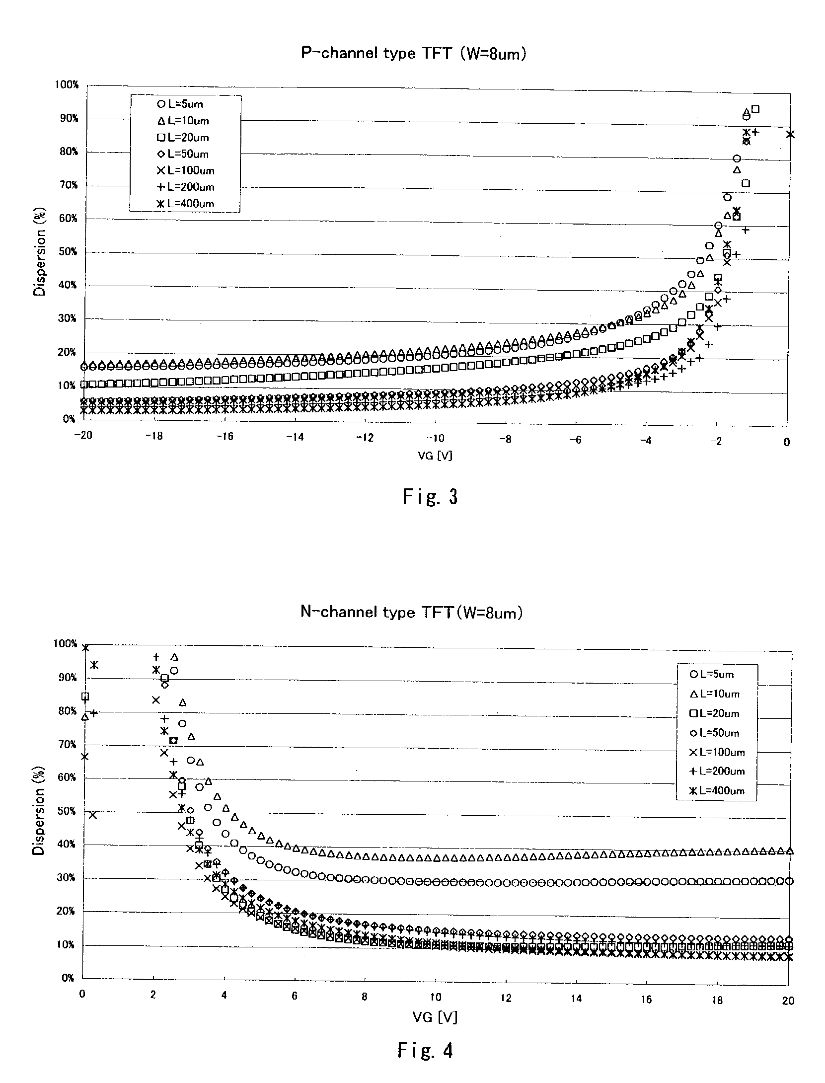
a technology of light-emitting devices and tft, which is applied in the direction of thermoelectric devices, identification means, instruments, etc., can solve the problems of increased driving voltage and power consumption, restricted aperture rate, and increased so as to reduce the current flow to the tft, the channel conductance gd is smaller, and the brightness constant

Inactive Publication Date: 2010-05-25
SEMICON ENERGY LAB CO LTD
View PDF159 Cites 70 Cited by
  • Summary
  • Abstract
  • Description
  • Claims
  • Application Information

AI Technical Summary

Benefits of technology

The present invention provides a pixel structure for an active matrix type light emitting device that raises the aperture rate in a pixel portion. The invention also addresses the issue of dispersion in the electric current value of the TFTs and proposes a solution to reduce the dispersion. The invention also introduces a TFT design with a longer channel length, which allows for a higher gate voltage and reduces the dispersion of the current value. The invention also discusses the importance of the threshold voltage in controlling the current value and proposes a method to set the threshold voltage to optimize the current value. Overall, the invention aims to improve the performance and efficiency of active matrix type light emitting devices.

Problems solved by technology

Moreover, in conventional active matrix type light emitting device, when resolution is tried to be raised, the problem that the aperture rate was restricted by arrangement of electrode for the retention capacitance in a pixel portion and the wiring for retention capacitance, TFT, various wiring, and the like had occurred.
It is regarded that when the Vth becomes larger, an increase in a driving voltage and in power consumption may be caused.

Method used


Image

  • Light emitting device having TFT
  • Light emitting device having TFT
  • Light emitting device having TFT

Examples


embodiment 1

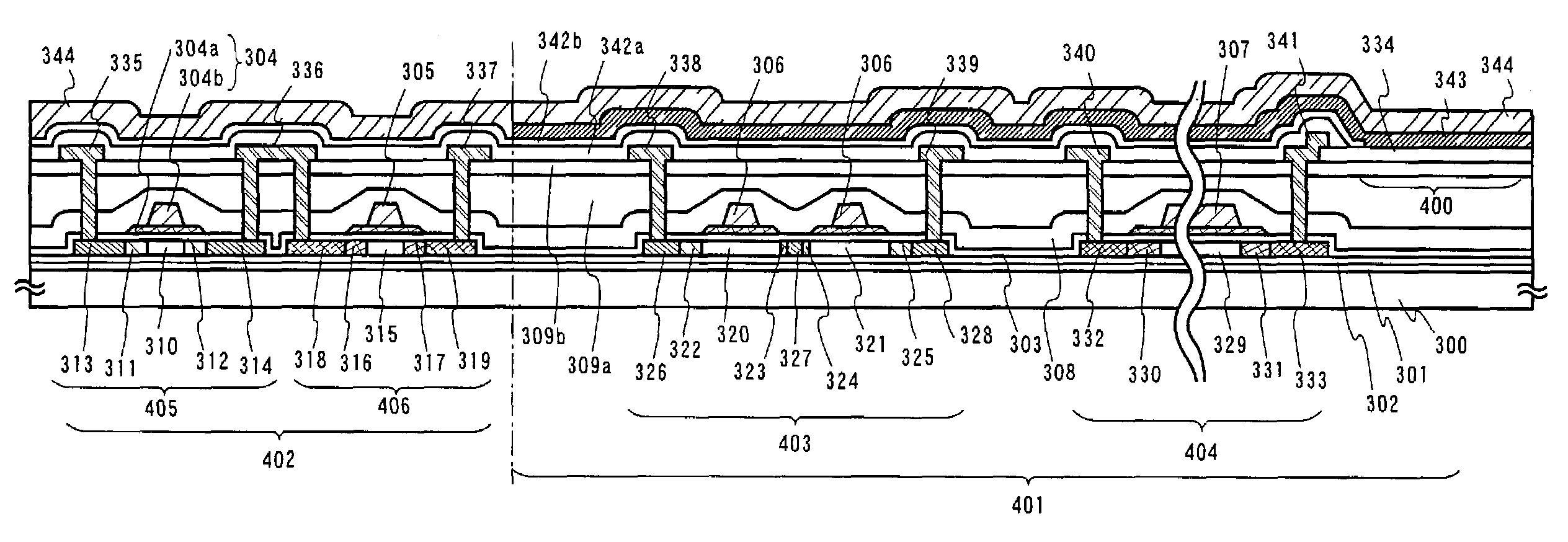
[0105]Here, a method of simultaneously manufacturing a pixel portion and TFTs (n-channel TFTs and a p-channel TFT) of a driving circuit provided in the periphery of the pixel portion over the same substrate to manufacture the light emitting device having OLED is described in detail.

[0106]For a lower layer of the base insulating film 301, a silicon oxynitride film formed from SiH4, NH3, and N2O as material gases (composition ratio: Si=32%, O=27%, N=24%, H=17%) is formed on the heat resistance glass substrate (the first substrate 300) having a thickness of 0.7 mm with a thickness of 50 nm (preferably 10 to 200 nm) and at a film deposition temperature of 400° C. by using plasma CVD. Then, after the surface is cleaned with ozone water, an oxide film on the surface is removed by means of dilute hydrofluoric acid (dilution with 1 / 100). Next, for an upper layer of a base insulating film 302, a silicon hydride oxynitride film formed from SiH4 and N2O as material gases (composition ratio: Si...

embodiment 2

[0150]This embodiment shows a top view (FIGS. 5 and 6) that is enlarged a part of the pixel portion in Embodiment 1, and a top view that is different in a part from FIGS. 5 and 6 is shown in FIGS. 13A and 13B.

[0151]FIG. 13A is a corresponding top view to FIG. 6, and same portions thereof are indicated by same symbols. FIG. 13A is an example of semiconductor layer 1102 that has different patterning shape that is adopted instead of the semiconductor layer 102 shown in FIG. 6. In this embodiment, the semiconductor layer 1102 is meandering. As shown in FIG. 13A, channel length L×channel width W is the same as FIG. 6, and is set 500 μm×4 μm. FIG. 13A is same as Embodiment 1 except the semiconductor layer 1102 that has a different patterning shape, so that another explanation may be referenced to Embodiment 1.

[0152]FIG. 13B shows another different top view. Same portion corresponding to FIG. 6 are indicated by same symbols. FIG. 13B shows a semiconductor layer 1202 that has different patt...

embodiment 3

[0154]The top view and cross-sectional view of the module type light emitting device (also referred to as EL module) obtained by Embodiment 1 or 2 are illustrated.

[0155]FIG. 6A is a top view of an EL module, and FIG. 14B is a cross-sectional view taken along the line A-A′ of FIG. 14A. In FIG. 14A, a base insulating film 501 is formed on a substrate 500 (for example, a heat resistant glass), and a pixel portion 502, a source driving circuit 504, and a gate driving circuit 503 are formed thereon. These pixel portion and driving circuit may be obtained by Embodiment 1 or 2.

[0156]Reference numeral 518 is an organic resin, reference numeral 519 is a protective film, a pixel portion and a driving circuit are covered with the organic resin 518, and the organic resin 518 is covered with the protective film 518. In addition, the cover material may be used to seal using bonding material. The cover material may be bonded as a support medium before peeled off.

[0157]Wiring 508 for transmitting s...


PUM


Abstract

The present invention provides a TFT that has a channel length particularly longer than that of an existing one, specifically, several tens to several hundreds times longer than that of the existing one, and thereby allowing turning to an on-state at a gate voltage particularly higher than the existing one and driving, and allowing having a low channel conductance gd. According to the present invention, not only the simple dispersion of on-current but also the normalized dispersion thereof can be reduced, and other than the reduction of the dispersion between the individual TFTs, the dispersion of the OLEDs themselves and the dispersion due to the deterioration of the OLED can be reduced.

Description

BACKGROUND OF THE INVENTION[0001]1. Field of the Invention[0002]The present invention relates to the manufacturing method of semiconductor device, in particular, present invention relates to a light emitting device comprising an organic light emitting device (OLED) formed over a substrate having an insulating surface. The invention also relates to an OLED module in which ICs including a controller, or the like, is mounted with an OLED panel. Note that, in this specification, the light emitting device includes the OLED panel and for the OLED module. Electronic equipment using the light emitting device is also included in the present invention.[0003]Noted that in the present specification, the term “semiconductor device” generally indicates a device which is capable of functioning by utilizing semiconductor characteristics, and a light emitting device, an electro-optical device, a semiconductor circuit and an electronic device are all included in the semiconductor device.[0004]2. Desc...

Claims


Application Information

Patent Timeline
Patent Type & Authority Patents(United States)
IPC IPC(8): H01L51/52H01L51/50G09F9/30H01L27/12H01L27/32H01L29/786H05B33/00
CPCH01L27/3262H01L29/78675H01L51/52H01L27/1222H01L29/78696H01L27/12H10K59/1213H05B33/00H10K50/80H10K59/131H01L27/124
Inventor UDAGAWA, MAKOTOHAYAKAWA, MASAHIKOKOYAMA, JUNOSAME, MITSUAKIANZAI, AYA
Owner SEMICON ENERGY LAB CO LTD
Learn More