Static and addressable emissive displays

a technology of emissive display and static, applied in the field of emissive display technology, to achieve the effect of significant durability and capability, high and unusual robustness, and higher variance within the tolerance of other printing

Active Publication Date: 2010-05-18
NTHDEGREE TECH WORLDWIDE
View PDF34 Cites 14 Cited by
  • Summary
  • Abstract
  • Description
  • Claims
  • Application Information

AI Technical Summary

Benefits of technology

[0017]As a light emitting display, the various embodiments of the invention have highly unusual properties. First, they may be formed by any of a plurality of conventional and comparatively inexpensive printing or coating processes, rather than through the highly involved and expensive semiconductor fabrication techniques, such as those utilized to make LCD displays, plasma displays, or alternating-current thin-film electroluminescent (“ACTFEL”) displays. The invention may be embodied using comparatively inexpensive materials, such as paper and phosphors (e.g., commercially available doped zinc sulfides, etc.), substantially reducing production costs and expenses. The ease of fabrication using printing processes, combined with reduced materials costs, may revolutionize display technologies and the industries which depend upon such displays, from computers to mobile telephones to financial exchanges.
[0019]In addition, the various embodiments provide a wide range of selectable resolutions and are highly and unusually robust under a wide variety of environmental conditions. The various exemplary embodiments also provide an electroluminescent display having sealed or encapsulated conductive and emissive regions, providing significant durability and capability to withstand a wide variety of environmental conditions and other sources of stress or degradation. The encapsulation techniques of the exemplary embodiments further allow packaging flexibility of the finished display; for example, the displays are not required to be separately sealed behind glass or plastic for consumer handling and use.
[0020]The various exemplary embodiments also provide an electroluminescent display having a substantially topologically uniform and printable surface, for direct application of an image to be illuminated. For example, the display surface may be formed to have both a surface chemically compatible with and suitable for conventional printing, and a surface having a topological variance of 4 microns or less, allowing for direct printing using virtually any printing technology, with a higher variance within tolerance for other printing technologies, such as screen printing. An exemplary electroluminescent display also provides for an optically or visually neutral density surface, for underlying layers to have negligible perceived visual effect. This has the further effect of eliminating any need for a separate masking or background layer found in prior art static electroluminescent displays.

Problems solved by technology

First, they may be formed by any of a plurality of conventional and comparatively inexpensive printing or coating processes, rather than through the highly involved and expensive semiconductor fabrication techniques, such as those utilized to make LCD displays, plasma displays, or alternating-current thin-film electroluminescent (“ACTFEL”) displays.

Method used


Image

  • Static and addressable emissive displays
  • Static and addressable emissive displays
  • Static and addressable emissive displays

Examples


example 1

Signage

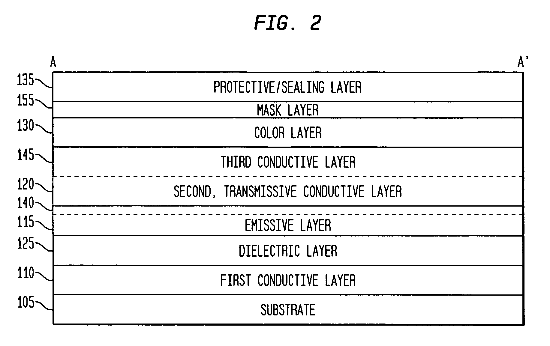
[0148]Using either continuous roll or sheeted substrate, a surface finish coating is applied, in order to smooth the surface of the substrate (on a micro or detailed level). A conductive ink is patterned on the “live” area of the substrate (i.e., the area to be illuminated) by offset printing, and allowed to dry as discussed above. Multiple applications of conductive ink are applied, using the alignment (reduced or choked patterning), and the remoisturizing discussed above. One or more dielectric layers are applied as a patterned coating on the area to be illuminated, and allowed to dry as discussed above. A polymer reflective (or mirror) layer is applied and cured through ultraviolet exposure, providing the plurality of reflective elements or interfaces. An emissive phosphor is applied as one or more patterned coatings on the area to be illuminated, and allowed to dry as discussed above. A clear ATO coating is applied as a patterned coating on the area to be illuminated, and...

example 2

Display

[0149]Also using either continuous roll or sheeted substrate, a surface finish coating is applied, in order to smooth the surface of the substrate (on a micro or detailed level). A conductive ink is patterned as rows (or columns) on this substrate surface using flexographic printing, and allowed to dry as discussed above. Multiple applications of conductive ink are applied, using the alignment (reduced or choked patterning), and the remoisturizing discussed above. One or more dielectric layers are applied as a coating bounded by the area of the active display, and allowed to dry as discussed above. A polymer reflective (or mirror) layer is applied and cured through ultraviolet exposure, providing the plurality of reflective elements or interfaces. An emissive phosphor is applied as one or more coatings bounded by (and slightly smaller than) the area of the active display of the dielectric layer (i.e., choked or slightly reduced area to be within the boundaries of the dielectr...


PUM


Abstract

The various embodiments of the invention provide an addressable or a static emissive display comprising a plurality of layers, including a first substrate layer, wherein each succeeding layer is formed by printing or coating the layer over preceding layers. Exemplary substrates include paper, plastic, rubber, fabric, glass, ceramic, or any other insulator or semiconductor. In an exemplary embodiment, the display includes a first conductive layer attached to the substrate and forming a first plurality of conductors; various dielectric layers; an emissive layer; a second, transmissive conductive layer forming a second plurality of conductors; a third conductive layer included in the second plurality of conductors and having a comparatively lower impedance; and optional color and masking layers. Pixels are defined by the corresponding display regions between the first and second plurality of conductors. Various embodiments are addressable, have a substantially flat form factor with a thickness of 1-3 mm, and are also scalable virtually limitlessly, from the size of a mobile telephone display to that of a billboard.

Description

CROSS-REFERENCE TO RELATED APPLICATIONS[0001]This application is a continuation-in-part of and claims priority to U.S. patent application Ser. No. 11 / 023,064, filed Dec. 27, 2004, inventors William Johnstone Ray et al., entitled “Addressable And Printable Emissive Display”, which are commonly assigned herewith, the contents of all of which are incorporated herein by reference, and with priority claimed for all commonly disclosed subject matter.[0002]This application is a continuation-in-part of and claims priority to U.S. patent application Ser. No. 11 / 181,488, filed Jul. 13, 2005, inventors William Johnstone Ray et al., entitled “Addressable And Printable Emissive Display”, which is a continuation of U.S. patent application Ser. No. 11 / 023,064, filed Dec. 27, 2004, inventors William Johnstone Ray et al., entitled “Addressable And Printable Emissive Display”, which are commonly assigned herewith, the contents of all of which are incorporated herein by reference, and with priority cl...

Claims


Application Information

Patent Timeline
Patent Type & Authority Patents(United States)
IPC IPC(8): H05B33/22H01J1/62
CPCG09G3/30G09G2300/0426H05B33/10H05B33/06H05B33/00
Inventor RAY, WILLIAM JOHNSTONELOWENTHAL, MARK DAVIDCLAYPOLE, TIMOTHY CHARLES
Owner NTHDEGREE TECH WORLDWIDE
Why Eureka
Try Eureka