
Sideband bus setting system and method thereof

a technology of sideband bus and setting system, which is applied in the field of sideband bus setting system, can solve the problems of master device, limitation of the number of target devices b>3/b>, and difficulty in implementing a consistent setting of all ics, so as to prevent the over-look of improper data setting

Inactive Publication Date: 2010-05-11
FUJITSU LTD
View PDF5 Cites 19 Cited by
  • Summary
  • Abstract
  • Description
  • Claims
  • Application Information

AI Technical Summary

Benefits of technology

This approach extends the number of connected target devices beyond address limitations, detects multiplexer failures proactively, and prevents improper data setting, ensuring reliable operation and reducing the risk of overlooked faults.

Problems solved by technology

Accordingly, it has become difficult to implement a consistent setting of all ICs through a main processor by using a main data path, and many ICs have a port for a sideband bus to perform the setting through a path different from the data path before the main processor starts access.
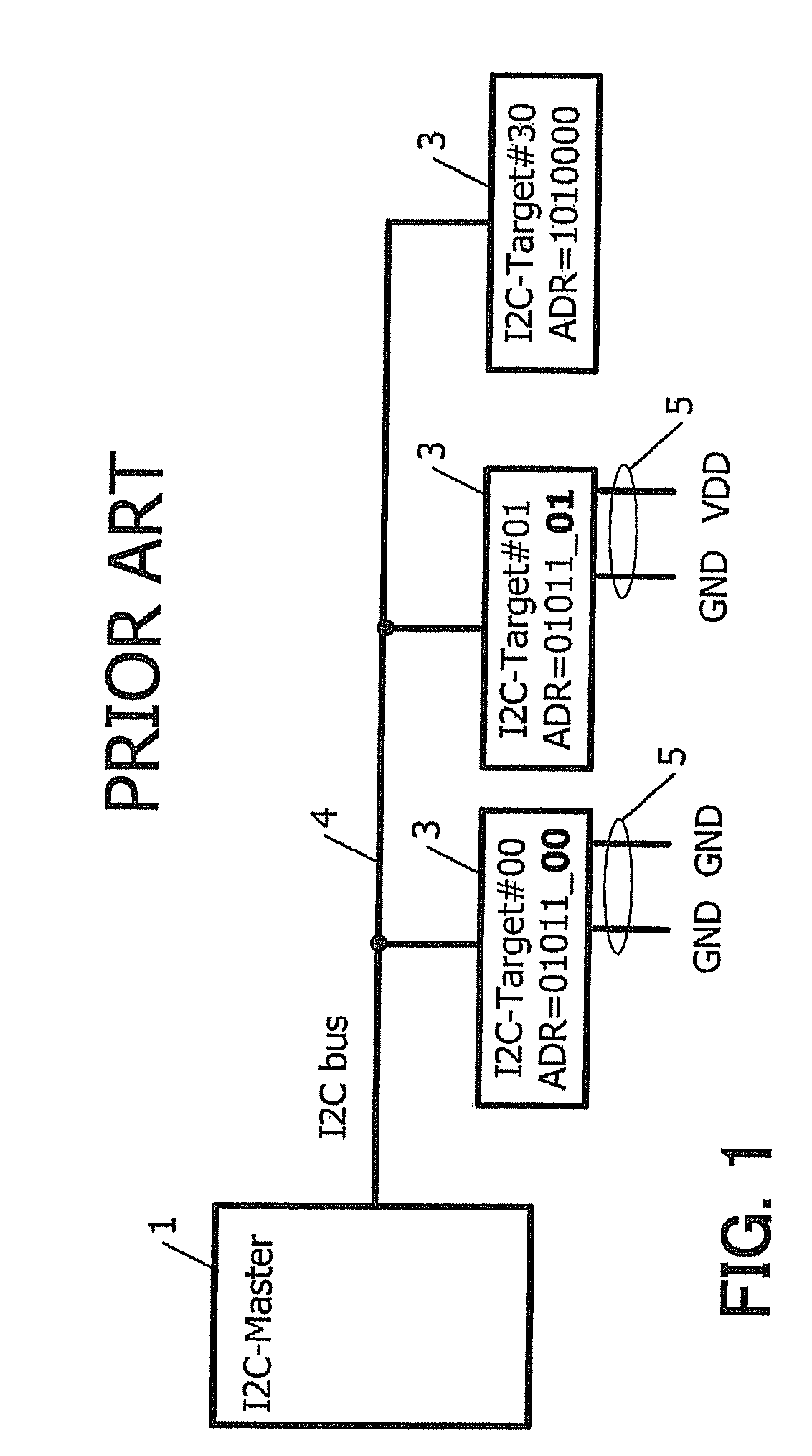
However, if the target device actually has only two bits for the address setting external pins, for example as shown in FIG. 1, there is a limitation that the number of target devices 3 coupled to the master device 1 through the sideband bus 4 is equal to or smaller than four (two raised to second power).

Method used


Image

  • Sideband bus setting system and method thereof
  • Sideband bus setting system and method thereof
  • Sideband bus setting system and method thereof

Examples


first embodiment

[0034]FIG. 3 illustrates an exemplary use of a sideband multiplexer according to the present invention.

[0035]Target devices 50 (#00-#01) are coupled to a master device 10 (I2C-Master 10) through a bus including a sideband multiplexer 2 (an I2C-MUX 2) and a side band bus 40 (I2C bus 40) connected to a target port CH0 of the I2C-MUX 2. A target device 53 (#30) is coupled to the master device 10 (I2C-Master 10) through a bus including the sideband multiplexer 2 (I2C-MUX 2) and a side band bus 43 (an I2C bus 43) connected to a target port CH2 of the I2C-MUX 2. Target devices 51 (#10-#13) are coupled to the master device 10 (I2C-Master 10) through a bus including the sideband multiplexer 2 (I2C-MUX 2) and a side band bus 41 (I2C bus 41) connected to a target port CH1 of the I2C-MUX 2. While, target devices 52 (#20-#23) are coupled to the target device 10 (I2C-Master 10) through a bus including a sideband multiplexer 2a (I2C-MUX 2a) and a side band bus 42 (I2C bus 42) connected to a targe...

second embodiment

[0041]FIG. 4 illustrates an exemplary configuration of a sideband bus setting system according to the present invention, in which many target devices are connected to a sideband multiplexer 2 (I2C MUX 2). In FIG. 4, it is assumed that target devices 51 (#10 to #13) and 52 (#20 to #23) are the ICs of the same type, and the target devices 51 and 52 form target domains 41a and 42a, respectively.

[0042]The target domains 41a and 42a are connected to the same I2C-MUX 2. The target devices 51 (#10-#13) connected to a target port CH1 of the I2C-MUX 2 and the target devices 52 (#20-#23) connected to a target port CH2 of the I2C-MUX 2 have the same device addresses respectively, but can exist because the target devices 51 (#10-#13) and 52 (#20-#23) belong to the different target domains 41a and 42a, respectively.

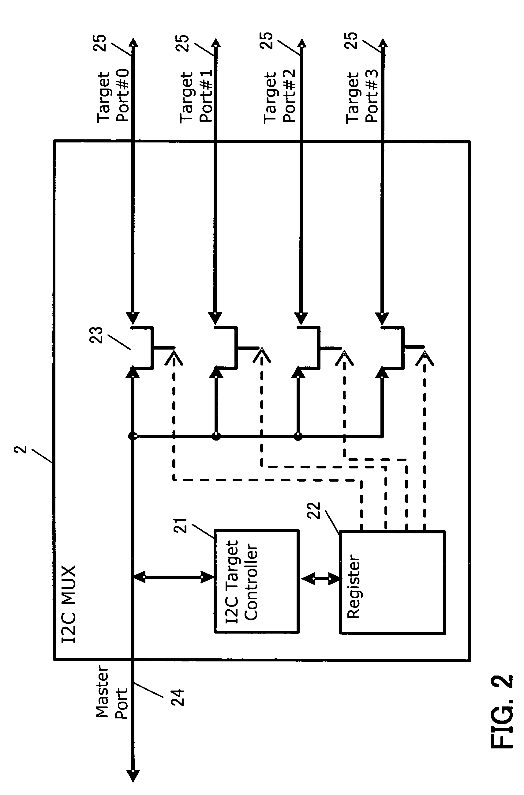
[0043]For example, when accessing from the master device 10 to #10 of the target device 51, first, the I2C-MUX 2 is accessed and the internal register 22 of the I2C-MUX 2 is set by th...


PUM


Abstract

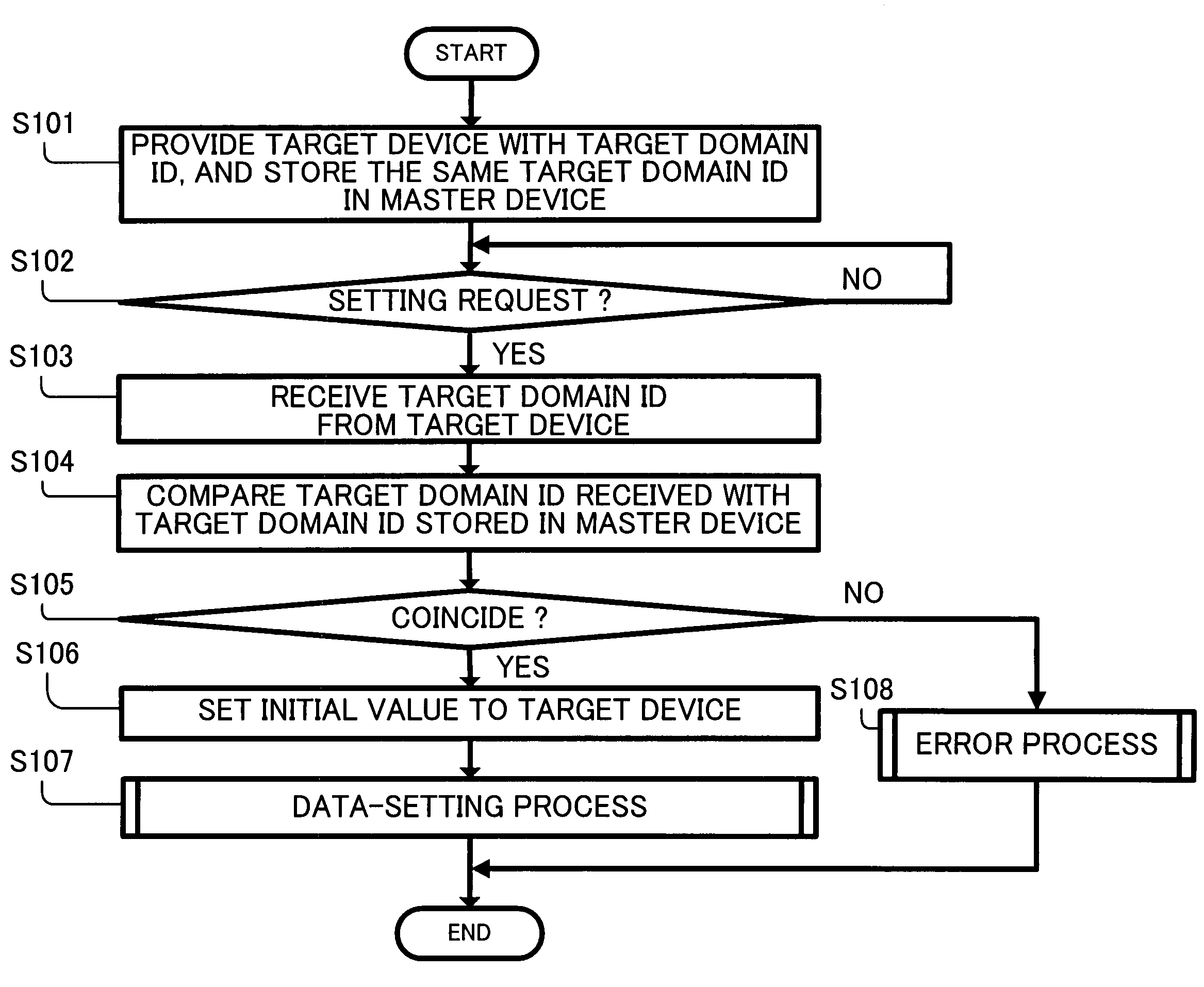
A sideband bus setting system in which multiple target devices (ICs) are communicably connected to a master device through a bus so as to set data to ICs mounted on an electronic device. The target device is provided with a target domain ID identifying a target domain-which is a subgroup of multiple target devices, and the master device is provided with the same target domain ID as that provided for the target device. The master device receives the target domain ID from the target device, and performs data-setting process to the target device when the target domain ID received from the target device coincides with the target domain ID provided for the master device. According to the above feature, the failure of the bus (for example, the failure of a sideband multiplexer) can be detected in advance, thereby preventing overlooking the improper data-setting operation.

Description

BACKGROUND OF THE INVENTION[0001]1. Field of the Invention[0002]The present invention relates to a sideband bus setting system used for setting an integrated circuit (IC) which is mounted on an electronic device, or for reading out the state of the IC.[0003]More particularly, the present invention has been made to configure the circuit to avoid that an improper setting of the IC or an improper readout of the state of the IC is performed by a sideband bus such as the Inter-Integrated Circuit (I2c) bus or the Two Wire Interface (TWI) due to an abnormal path.[0004]2. Description of the Related Art[0005]As the size of a computer such as a server has increased, the types and the number of ICs which are mounted on a unit of the computer have increased. Accordingly, it has become difficult to implement a consistent setting of all ICs through a main processor by using a main data path, and many ICs have a port for a sideband bus to perform the setting through a path different from the data ...

Claims


Application Information

Patent Timeline
Patent Type & Authority Patents(United States)
IPC IPC(8): H04J3/04
CPCG06F13/4226
Inventor OHARA, SHIGEYOSHI
Owner FUJITSU LTD
Learn More