Laser processing apparatus and laser processing method for cutting and removing a part of a surface region of a substrate
a laser processing and surface region technology, applied in metal working equipment, manufacturing tools, instruments, etc., can solve the problems of increasing manufacturing costs and weight of laser processing equipment, unable to cut resist films formed on work, and disadvantage of apparatus
- Summary
- Abstract
- Description
- Claims
- Application Information
AI Technical Summary
Benefits of technology
Problems solved by technology
Method used
Image
Examples
first embodiment
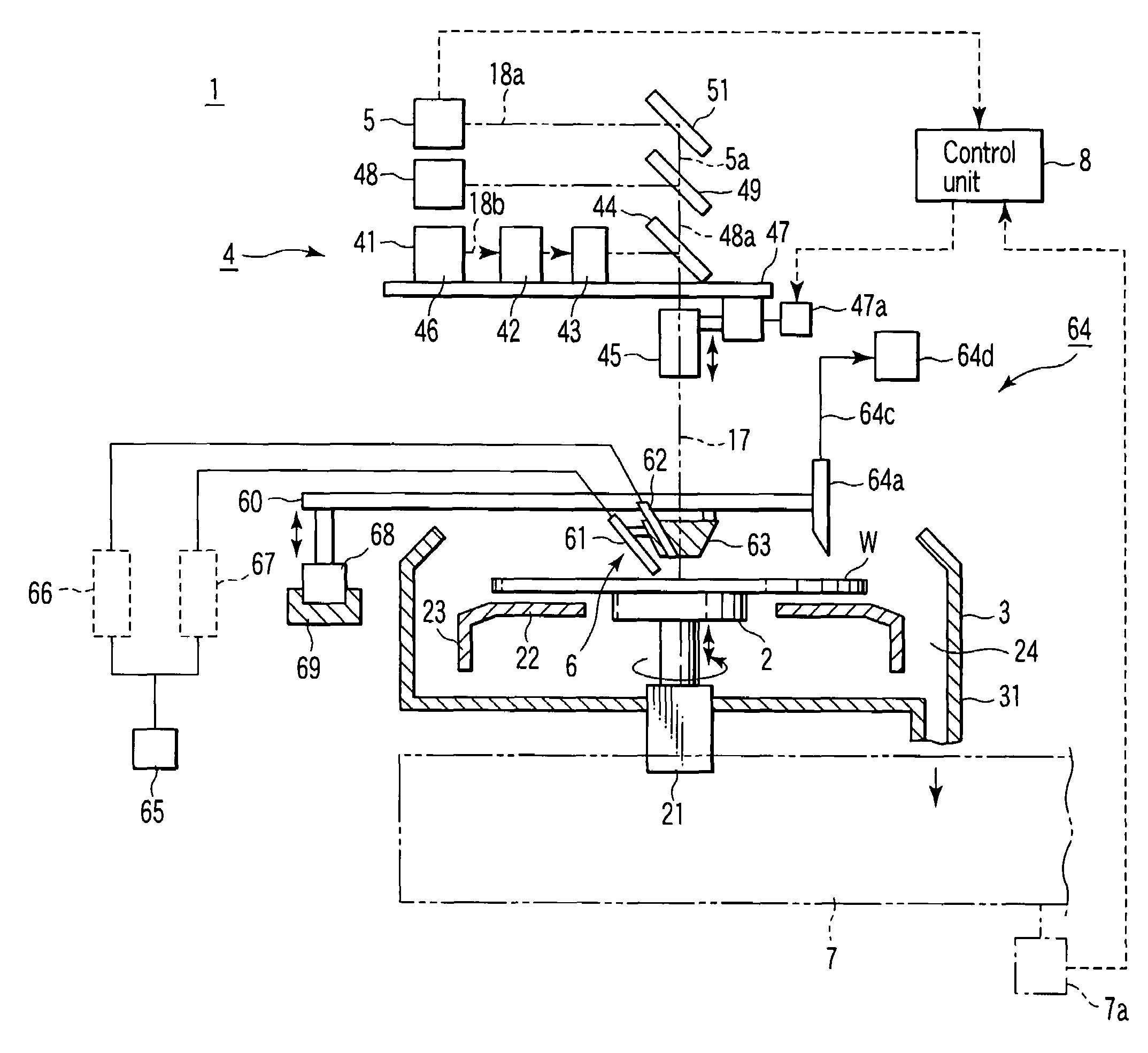
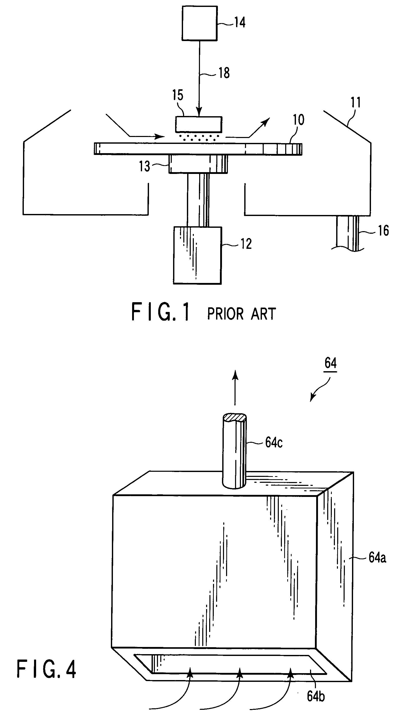
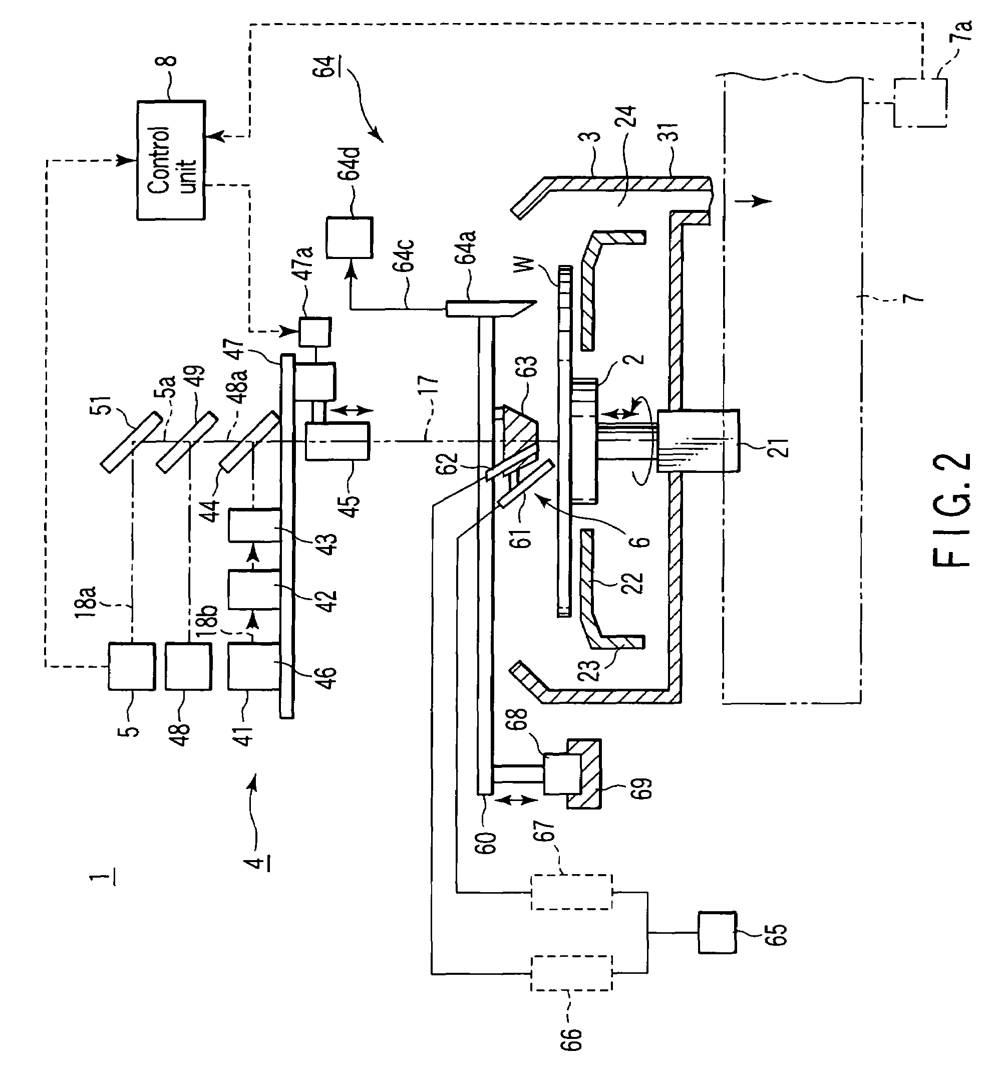
[0051]FIG. 2 is a diagram illustrating a laser processing apparatus according to an embodiment of this invention. The laser processing apparatus 1 is used in various processes such as dicing and processing of thin films. More specifically, the apparatus 1 can process various thin films such as insulating film, metal film and resist film, can form dicing lines and can remove a resist film from alignment marks to expose the marks to light. The apparatus 1 has a spin chuck 2, a cup 3 and a drive unit 21. The spin chuck 2 is a substrate-holding unit for holding a wafer W by suction, keeping the wafer W in a horizontal position. The chuck 2 is arranged in the cup 3, which is shaped like a hollow cylinder. The drive unit 21 rotates the spin chuck 2 around a vertical axis (Z-axis) and moves the spin chuck 2 up and down along the Z-axis.
[0052]The cup 3 has an outlet port (liquid-discharging port) 31 made in the bottom and located near the circumference of the bottom. Through the outlet port...
second embodiment
[0094]A second embodiment of this invention will be described, with reference to FIG. 14.
[0095]In the second embodiment, the laser displacement meter 5 and the half-mirror 51 are so positioned that the laser displacement meter 5 has its optical axis 5a lies in front of the axis 17 of the laser beam 18b, with respect to the process direction of the arrow shown in FIG. 14. Except for this point, the second embodiment is identical in structure to the first embodiment. The term “process direction” means the direction in which spot of the laser beam 18b moves on the surface of the wafer W.
[0096]As in the first embodiment described above, the wafer W is transferred to the chuck 2 and set in a desired position, and the laser process is carried out, while adjusting the height of the optical unit 45. More precisely, the X-Y stage 7 moves the wafer W until the dicing-starting point on the wafer W comes into alignment with the optical axis 17 of the laser unit 4.
[0097]Subsequently, the support...
third embodiment
[0101]A third embodiment of this invention will be described, with reference to FIG. 15. The components identical to those of the first and second embodiments will not be described.
[0102]The third embodiment has an additional laser displacement meter 9 for detecting the depth of a recess made in the surface of the wafer W during the laser process. The laser displacement meter 9 is emits a distance-measuring laser beam 18c to the wafer W. The laser displacement meter 9 may be so positioned that the laser beam 18c travels at the back of the axis 17 of the wafer-processing laser beam emitted from the laser source 41.
[0103]In the present embodiment, the laser displacement meter 9 emits a distance-measuring laser beam 18c immediately after a wafer-processing laser beam 28b is applied to processing point PN. The surface of the wafer W reflects the distance-measuring laser beam 18c. From the laser beam 18c reflected, the depth of the recess formed in the surface of the wafer W. If the dept...
PUM
| Property | Measurement | Unit |
|---|---|---|
| focal distance | aaaaa | aaaaa |
| wavelength | aaaaa | aaaaa |
| wavelength | aaaaa | aaaaa |
Abstract
Description
Claims
Application Information
 - R&D
- Intellectual Property
- Life Sciences
- Materials
- Tech Scout
- Unparalleled Data Quality
- Higher Quality Content
- 60% Fewer Hallucinations
Browse by: Latest US Patents, China's latest patents, Technical Efficacy Thesaurus, Application Domain, Technology Topic, Popular Technical Reports.
© 2025 PatSnap. All rights reserved.Legal|Privacy policy|Modern Slavery Act Transparency Statement|Sitemap|About US| Contact US: help@patsnap.com


