Method for fabricating pixel structure

a technology of pixel structure and fabrication method, which is applied in the direction of basic electric elements, electrical apparatus, semiconductor devices, etc., can solve the problems of high probability of defects in the pixels of poly-si tft, high cost of manufacturing, and complex methods for fabricating pixels. the effect of low manufacturing cos

Active Publication Date: 2010-04-20
AU OPTRONICS CORP
View PDF9 Cites 2 Cited by
  • Summary
  • Abstract
  • Description
  • Claims
  • Application Information

AI Technical Summary

Benefits of technology

[0008]Accordingly, the present invention is directed to a method for fabricating a pixel structure for reducing the manufacturing cost.
[0019]The present invention integrates two photolithography and etching processes for fabricating the patterned dielectric layer and the source / drain and adopts less photolithography and etching processes. The method for fabricating a pixel structure according to the present invention can not only save the cost of the photo-masks, but also decrease the defects caused by the complex processes.

Problems solved by technology

The method for fabricating pixels having the low-temperature poly-Si TFT is complex.
Therefore, the conventional method for fabricating the pixels of the low-temperature poly-Si TFT generally needs about eight or nine photolithography and etching processes, and the steps of this fabricating method are complex and quite time consuming.
The complex fabricating steps result in higher probability of defects in the pixels of the poly-Si TFT, and the low production yield.
Furthermore, the conventional method for fabricating the pixel having the low-temperature poly-Si TFT adopts more fabricating steps and requires longer fabricating time.
Therefore, the total cost of production is added due to the increase of the cost for purchasing machines and equipments and the material cost for production.

Method used


Image

  • Method for fabricating pixel structure
  • Method for fabricating pixel structure
  • Method for fabricating pixel structure

Examples


Embodiment Construction

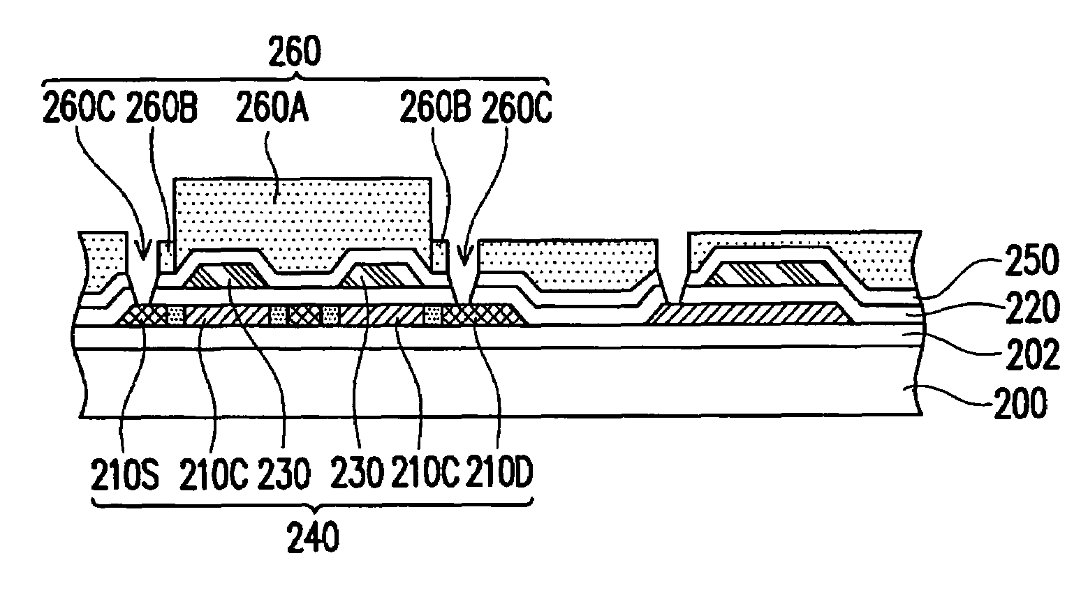
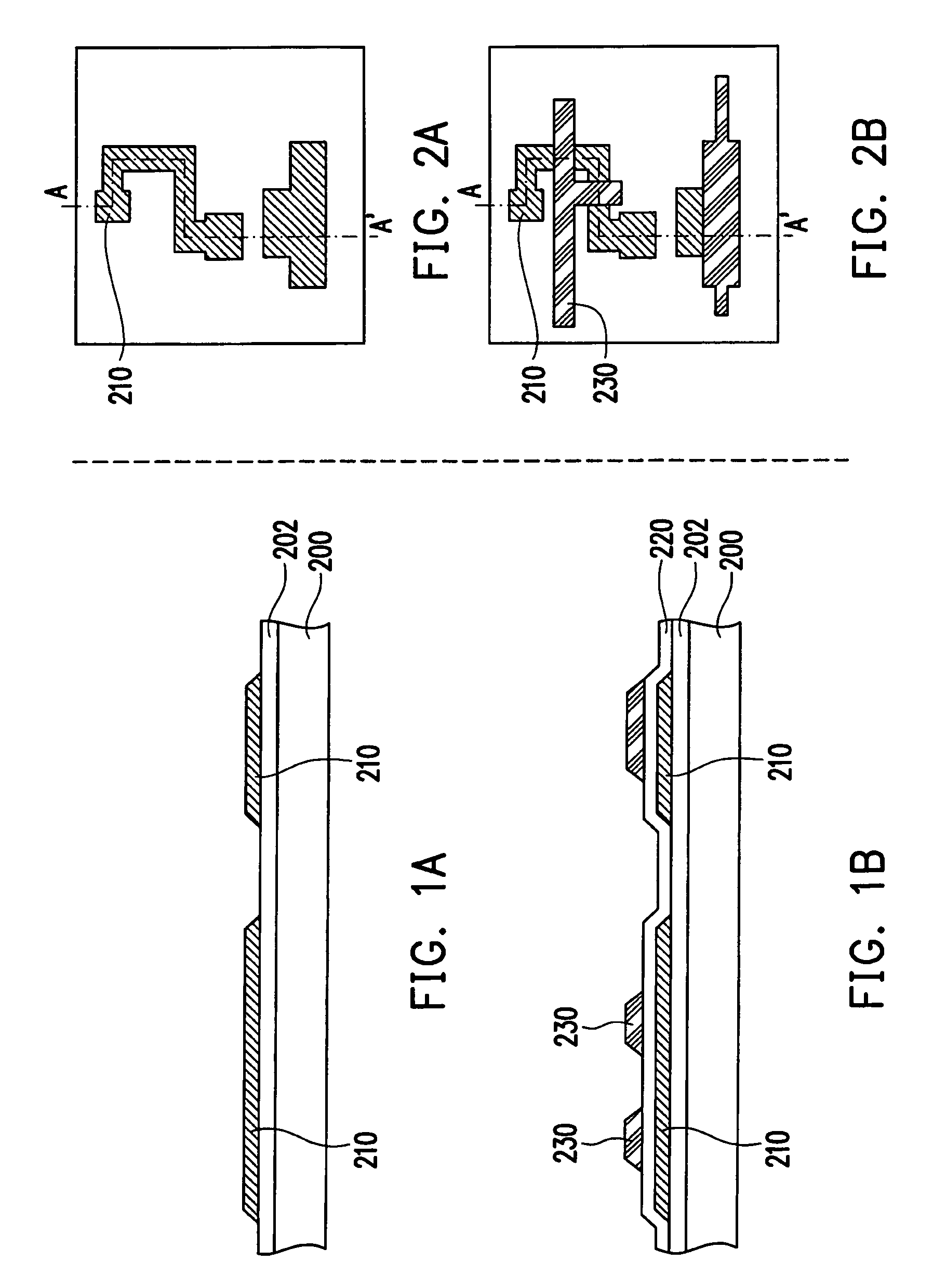
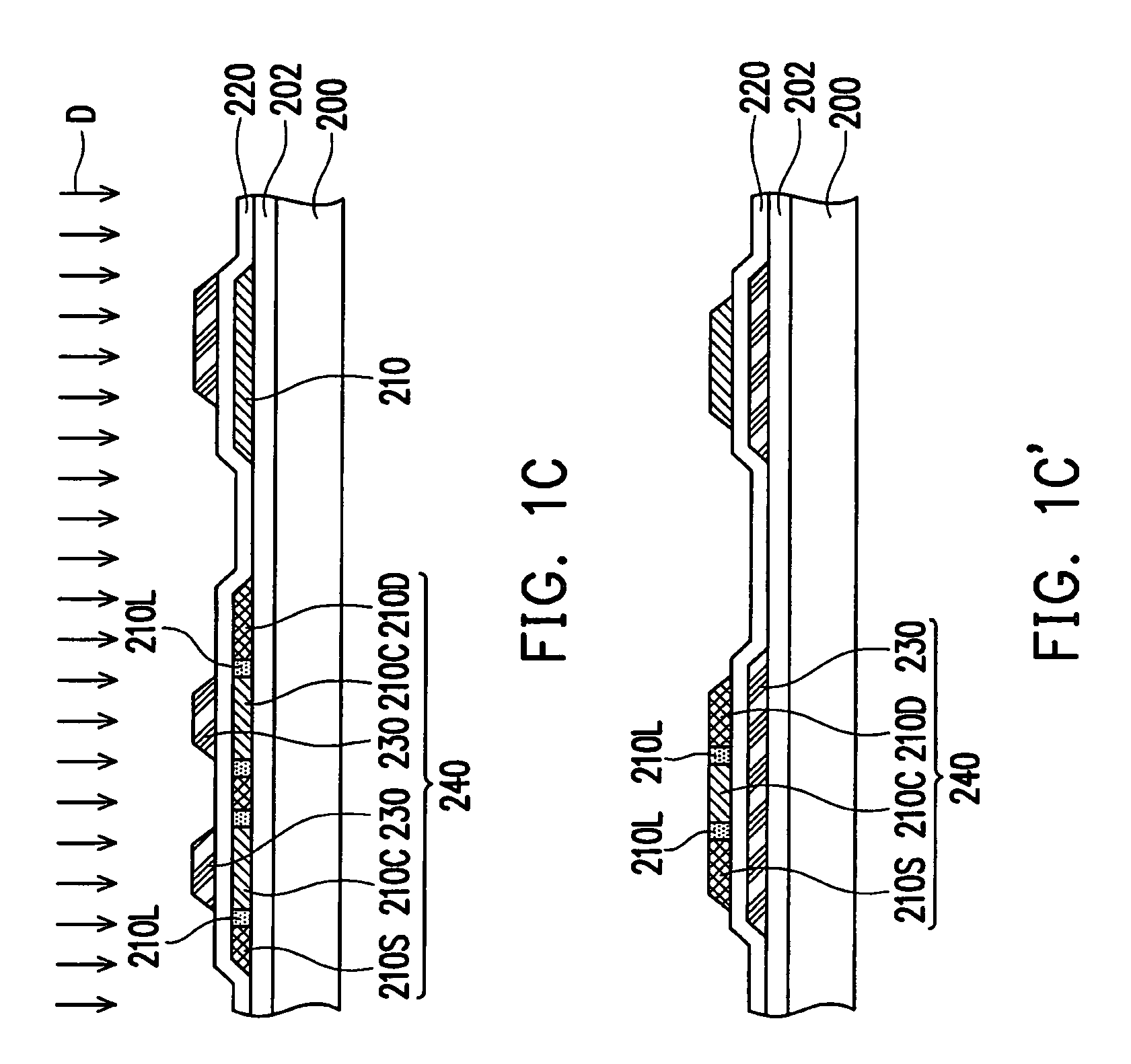
[0027]FIGS. 1A to 1I are schematic cross-sectional views for illustrating a method for fabricating a pixel structure of the present invention. Referring to FIG. 1A, first, a substrate 200 is provided, and the substrate 200 is, for example, a rigid substrate or a flexible substrate, such as, glass substrate or plastic substrate. Then, a semiconductor layer 210 is formed on the substrate 200. In this embodiment, the method for forming the semiconductor layer 210 includes the following steps. First, a semiconductor material layer (not shown) is formed on the substrate 200. Then, the semiconductor material layer is patterned by a photolithography process and an etching process, so as to form a semiconductor layer 210. FIG. 2A is a top view of FIG. 1A, and FIG. 1A is a cross-sectional view taken along a section line of A-A′ of FIG. 2A. In addition, the material of the semiconductor layer 210 is, for example, poly-silicon or doped poly-silicon.

[0028]In this embodiment, before forming the ...


PUM


Abstract

A method for fabricating a pixel structure is provided. First, a substrate having an active device formed thereon is provided. The active device has a gate, a gate dielectric layer, and a semiconductor layer having a channel, a source, and a drain region. Then, a dielectric layer is formed to cover the active device, and a photo-resist layer having a first photo-resist block and a second photo-resist block thinner than the first photo-resist block is formed on the dielectric layer. The second photo-resist block has openings above the source and the drain region, respectively. The source and the drain regions are exposed by removing part of the dielectric layer with the photo-resist layer as a mask. A second metal layer is formed after removing the second photo-resist block. A source and a drain are formed after removing the first photo-resist block. A pixel electrode connected to the drain is formed.

Description

CROSS-REFERENCE TO RELATED APPLICATION[0001]This application claims the priority benefit of Taiwan application serial no. 96133056, filed on Sep. 5, 2007. The entirety of the above-mentioned patent application is hereby incorporated by reference herein and made a part of this specification.BACKGROUND OF THE INVENTION[0002]1. Field of the Invention[0003]The present invention relates to a method for fabricating a pixel structure. More particularly, the present invention relates to a method for fabricating a pixel structure with reduced number of photolithography and etching processes (PEPs).[0004]2. Description of Related Art[0005]Displays are communication interfaces between human and information, while flat panel displays are the current trend. The flat panel displays may be divided into the following categories: organic electroluiminescence displays, plasma display panels (PDPs), and TFT-LCDs, and so on. Low-temperature poly-Si TFT LCDs, advantageous in thin thickness, light weight...

Claims


Application Information

Patent Timeline
Patent Type & Authority Patents(United States)
IPC IPC(8): H01L21/44
CPCH01L27/1214H01L27/1288
Inventor CHENG, YI-SHENGTSAI, CHIA-CHI
Owner AU OPTRONICS CORP
Why Eureka
Try Eureka