Area efficient and fast static random access memory circuit and method

a static random access and circuit technology, applied in static storage, information storage, digital storage, etc., can solve the problems of increasing the test time, increasing the die area, and increasing the power consumption

Inactive Publication Date: 2010-03-23
MONTEREY RES LLC
View PDF6 Cites 6 Cited by
  • Summary
  • Abstract
  • Description
  • Claims
  • Application Information

AI Technical Summary

Benefits of technology

[0016]According to a third aspect of the present invention, a method of recording an occurrence of sampled data in a device under test, includes steps of: (a) reading data stored in a memory unit at an address; (b) modifying the data to generate accumulated data, wherein step (b) is performed internally to the memory unit; and writing the incremented data to the address, wherein steps (a), (b), and (c) are performed in no more than a single clock cycle.

Problems solved by technology

Thus, multiple clock sub cycles are required for performing read, modify and write operations, which is a disadvantage in the conventional system.
A disadvantage of the conventional method is that the SRAM block 104 cannot perform increment or decrement operations internally, hence the increment and decrement operations are done externally by the ASIC block 102.
The process requires read, write and modify operations to complete one increment operation, which requires multiple clock cycles, thereby increasing the testing time.
Another disadvantage of conventional method is that an extra circuit and an extra SRAM is required for overflow protection, thereby adding to die area and adding to the power consumption.

Method used


Image

  • Area efficient and fast static random access memory circuit and method
  • Area efficient and fast static random access memory circuit and method
  • Area efficient and fast static random access memory circuit and method

Examples


Embodiment Construction

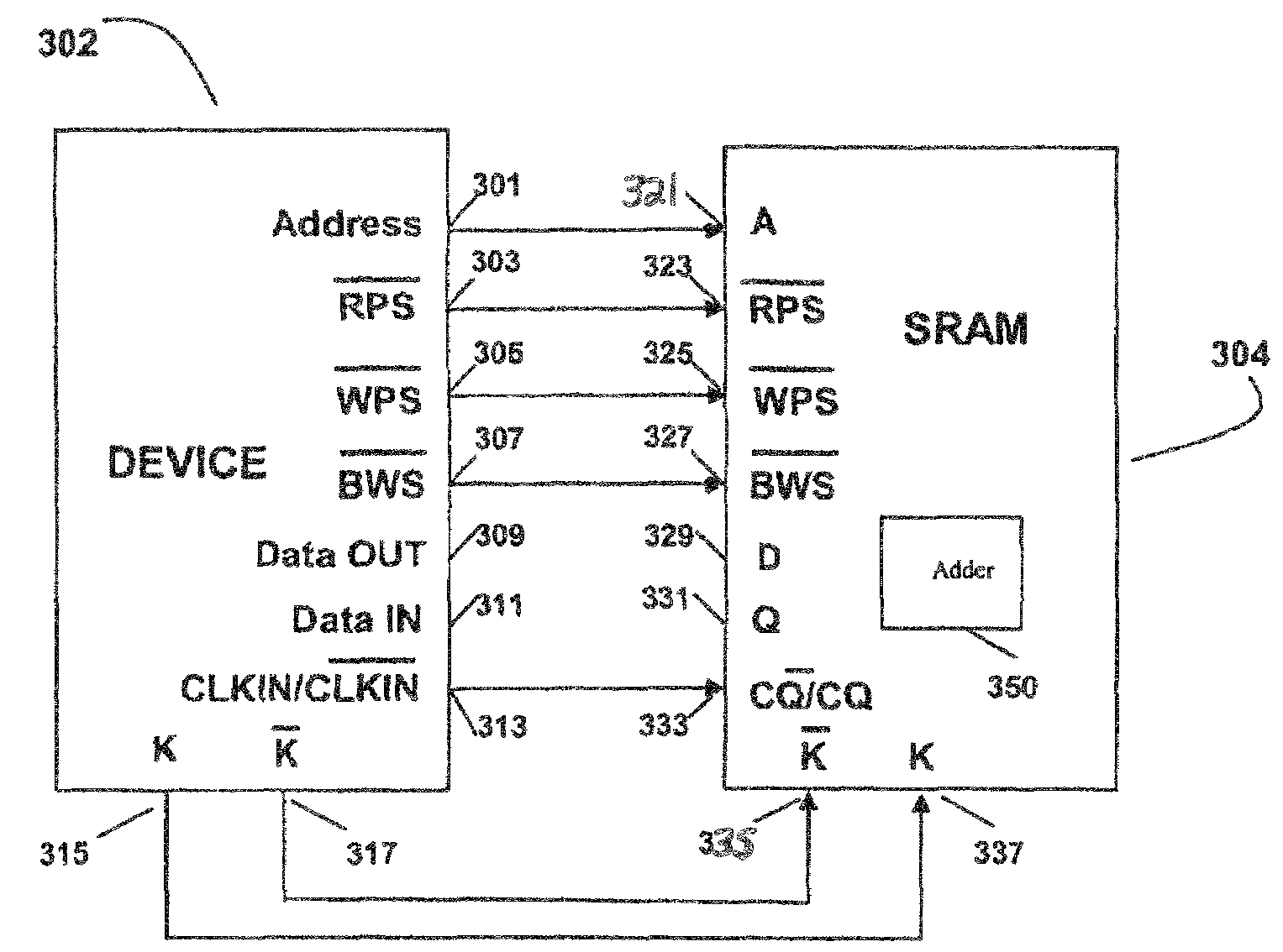
[0025]Exemplary embodiments of the present invention are directed to an efficient and a fast static random access memory circuit and method. The improved circuit provides fast read, write and modify operations in a single clock cycle time, which can be used for a fast and efficient testing methodology. However, the present invention is not restricted to a static random access memory. In an embodiment of the invention, the improved system comprises a memory unit, wherein the memory unit comprises a plurality of storage matrices further comprising an accumulation device; and a logic unit, wherein the logic unit comprises a register unit coupled to each storage matrix of the memory unit in a single cycle read, modify and write configuration. The accumulation device comprises a reconfigurable adder circuit performing read, modify and write operations in a single clock cycle. The improved system provides data overflow protection with no additional requirement for external adders and extr...


PUM


Abstract

Disclosed is an accumulation memory circuit for providing a fast read, modify, and write operation in a single clock cycle time. The memory circuit is configured to read data stored in the memory device at an address. The memory circuit includes a reconfigurable adder unit generating read, accumulate and write output in a single clock cycle. The memory circuit is further configured to minimize data overflow. A high speed accumulation method comprises resetting a memory circuit; reading from an address of the memory circuit; performing internal addition within the memory circuit and rewriting into the address of the memory circuit in a single clock cycle.

Description

[0001]This application claims priority under 35 U.S.C. §119(e) to U.S. Provisional Application No. 60 / 874,993, filed on Dec. 15, 2006, the entire contents of which are hereby incorporated by reference herein.BACKGROUND[0002]1. Field of the Invention[0003]The present invention relates to semiconductor memory devices. More particularly, the present invention relates to an efficient and a fast SRAM circuit and method providing for read, modify, and write operations in a single clock cycle time.[0004]2. Background Information[0005]A conventional Static Random Access Memory (SRAM) is a form of electronic data storage which retains data as long as power is supplied. Random access means that locations in the memory can be written to or read from in any order, regardless of the memory location that was last accessed. SRAM memory is widely utilized in electronic devices, and is particularly well-suited for use in portable or hand-held applications where low power consumption is required. SRA...

Claims


Application Information

Patent Timeline
Patent Type & Authority Patents(United States)
IPC IPC(8): G11C7/00G11C7/10
CPCG11C11/413G11C7/1006
Inventor LEE, CHRISTOPHERTRAN, THINHTZOU, JOSEPHWHATELY, MORGAN
Owner MONTEREY RES LLC
Why Eureka
Try Eureka