Substrate processing system for setting uniform module cycle length and access control time lag in two pipeline processing systems
a processing system and substrate technology, applied in the direction of program control, instrumentation, total factory control, etc., can solve the problems of unoptimized transfer procedure, adverse effects on the entire system, and insufficient optimization of the transfer process
- Summary
- Abstract
- Description
- Claims
- Application Information
AI Technical Summary
Benefits of technology
Problems solved by technology
Method used
Image
Examples
first embodiment
Substrate Processing System Achieved in the First Embodiment
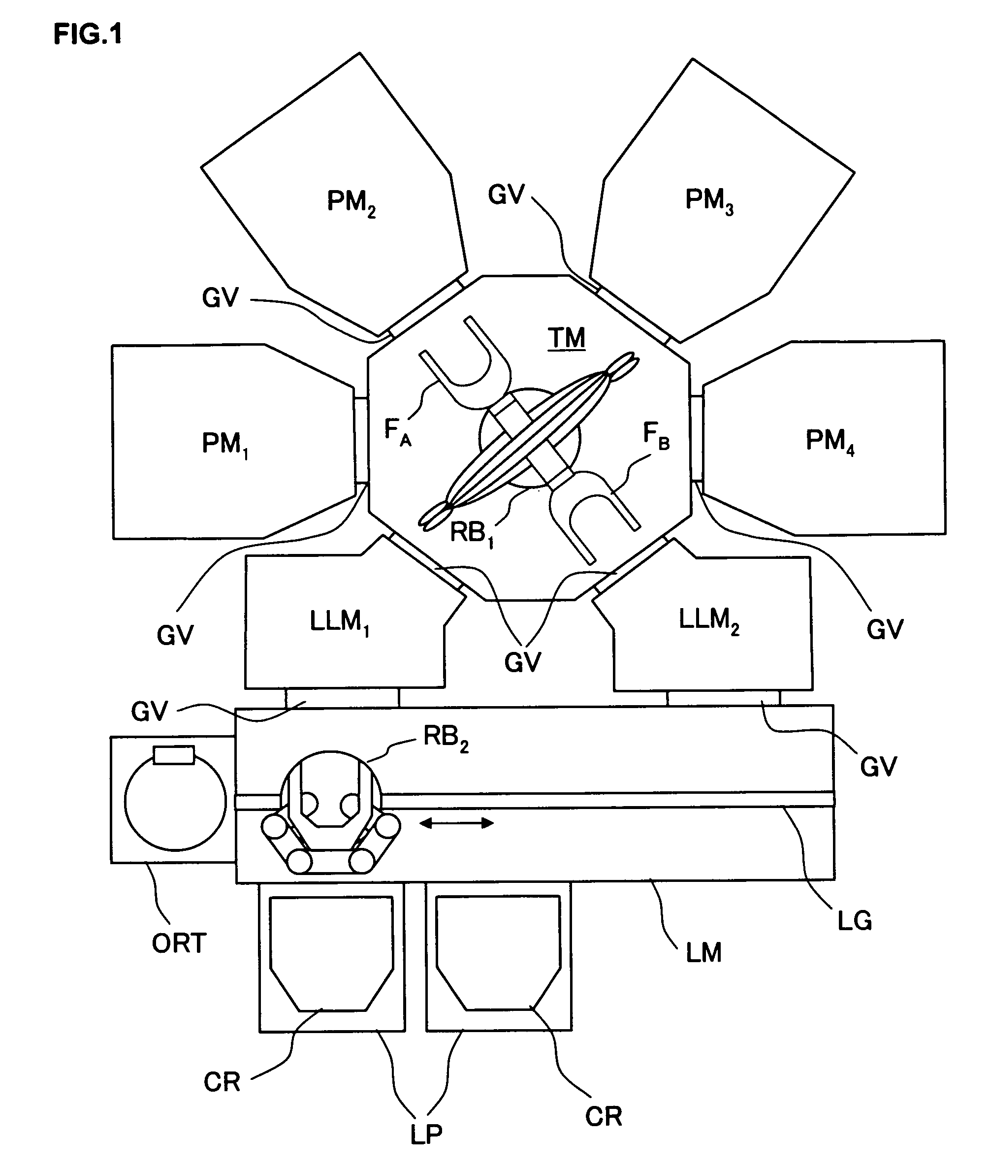
[0051]First, the substrate processing system achieved in the first embodiment of the present invention is explained in reference to drawings. FIG. 1 schematically shows the structure adopted in the substrate processing system achieved in the first embodiment. This substrate processing system includes a cluster tool (multichamber apparatus) achieved by connecting a plurality (e.g., four) of process modules (processing devices) PM1, PM2, PM3 and PM4 and two load-lock modules (load-lock chambers) LLM1 and LLM2 around a transfer module (vacuum transfer chamber) TM. The transfer module TM disposed at a substantial center of the cluster tool is connected with the individual modules PM1, PM2, PM3, PM4, LLM1 and LLM2 via gate valves GV each of which can be opened / closed freely.
[0052]The process modules each include a processing chamber (or a vacuum chamber) in which the pressure can be reduced to achieve a desired degree of vacuum....
first implementation example
of the Transfer Sequence
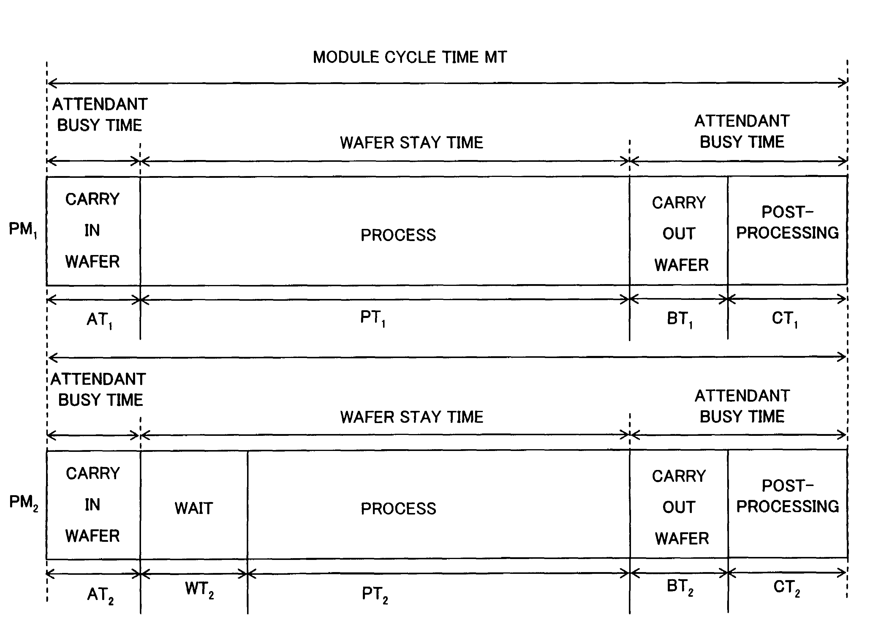
[0101]Next, the first implementation example of a transfer sequence that may be executed in conformance to the substrate processing program described above in the substrate processing system achieved in the embodiment is explained. FIG. 5 presents a specific example of the transfer sequence. Through the transfer sequence achieved in the first implementation example, a batch of wafers A (e.g., a predetermined number of wafers A01 through Anm) corresponding to a single cassette capacity, which have been loaded at a load port LP in the substrate processing system shown in FIG. 1, are sequentially transferred one wafer at the time, to the plurality of process modules PM1 and PM2 and the wafers A01 through Anm individually undergo a series of processing.
[0102]The shaded areas in FIG. 5 each indicate an active period of time (e.g., a period of time over which a wafer is being transferred during the wafer transfer processing, a period of time during which a wafer is...
second implementation example
of the Transfer Sequence
[0146]Next, the second implementation example of a transfer sequence that may be executed in conformance to the substrate processing program described above in the substrate processing system achieved in the embodiment is explained.
[0147]While only the process modules PM1 and PM2 in the cluster tool are engaged in operation and the other process modules PM3 and PM4 are not engaged in operation in the transfer sequence in the first implementation example explained above in reference to FIG. 5, all the process modules PM1, PM2, PM3 and PM4 in the cluster tool are simultaneously engaged in operation in the second implementation example.
[0148]The transfer sequence achieved in the second implementation example is shown in FIG. 7. The second implementation example is a specific example of a transfer sequence through which processing in a first pipeline processing system and processing in a second pipeline processing system are executed concurrently.
[0149]In the fir...
PUM
 Abstract
Description
Claims
Application Information
 - R&D
- Intellectual Property
- Life Sciences
- Materials
- Tech Scout
- Unparalleled Data Quality
- Higher Quality Content
- 60% Fewer Hallucinations
Browse by: Latest US Patents, China's latest patents, Technical Efficacy Thesaurus, Application Domain, Technology Topic, Popular Technical Reports.
© 2025 PatSnap. All rights reserved.Legal|Privacy policy|Modern Slavery Act Transparency Statement|Sitemap|About US| Contact US: help@patsnap.com


