2-write 3-read SRAM design using a 12-T storage cell

Active Publication Date: 2009-12-01
CALDER GROUP +1
View PDF5 Cites 18 Cited by
  • Summary
  • Abstract
  • Description
  • Claims
  • Application Information

AI Technical Summary

Benefits of technology

[0010]One advantage of the disclosed SRAM storage cell is that the write word line operates at twice the clock frequency, and the write bit lines are differential to provide high-performance writes. Each read word line operates at the clock frequency, and single-ended read bit lines are used to provide read performance comparable to write performance. The resulting storage cell only requires four horizontal word lines and five vertical bit lines, thereby enabling very dense, yet high-performance designs.

Problems solved by technology

This configuration typically requires more die area for the word lines and bit lines used to connect SRAM cells than the actual transistors used to compose the SRAM cells, resulting in relatively low die area utilization within the SRAM circuit.
However, minimizing die area is an important requirement because die area directly impacts the cost of manufacturing a given integrated circuit.
However, multiplexing access to an SRAM circuit may not meet certain performance requirements and is not a suitable solution in many cases.

Method used


Image

  • 2-write 3-read SRAM design using a 12-T storage cell
  • 2-write 3-read SRAM design using a 12-T storage cell
  • 2-write 3-read SRAM design using a 12-T storage cell

Examples


Embodiment Construction

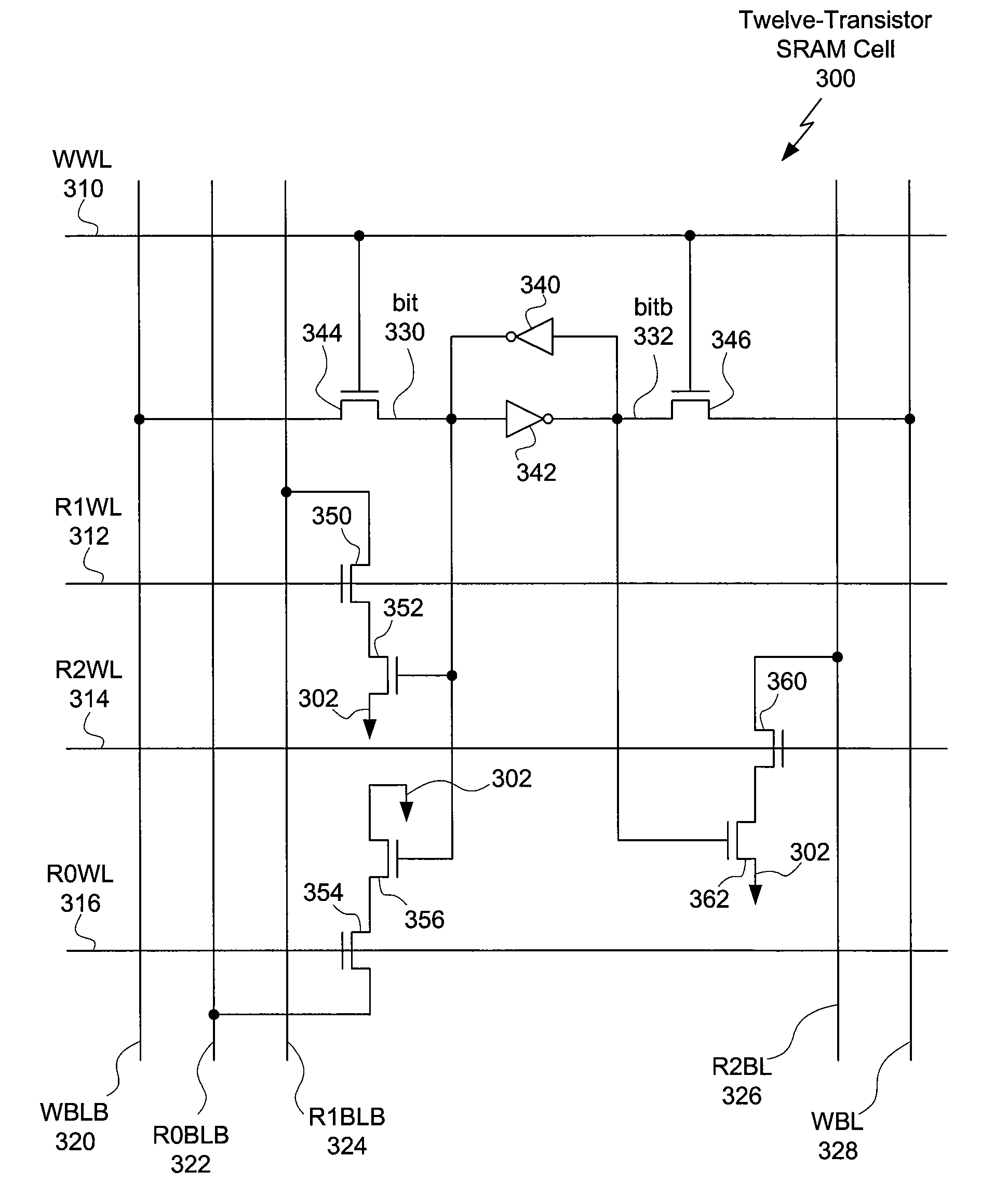
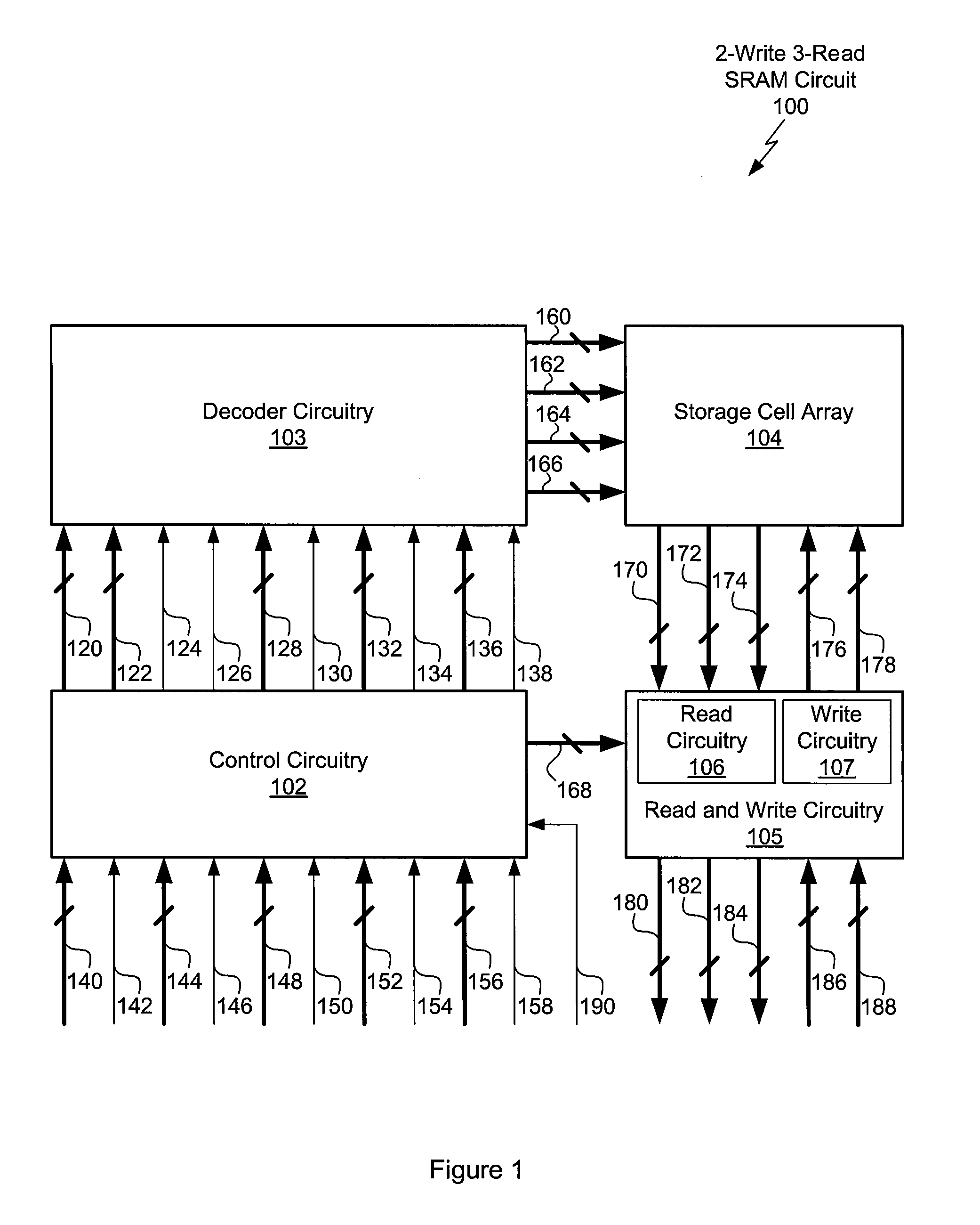
[0026]FIG. 1 illustrates the architecture of a two write (2-write), three read (3-read) static random access (SRAM) memory circuit 100, according to one embodiment of the invention. The 2-write 3-read SRAM circuit 100 includes control circuitry 102, decoder circuitry 103, a storage cell array 104, and read and write circuitry 105.

[0027]The control circuitry 102 includes two input write addresses, write address zero (W0A) 140 and write address one (W1A) 144, with corresponding write enables write enable zero (W0E) 142 and write enable one (W1E) 146. The control circuitry 102 also includes three input read addresses, read address zero (R0A) 148, read address one (R1A) 152 and read address two (R2A) 156, with corresponding read enables read enable zero (R0E) 150, read enable one (R1E) 154, and read enable two (R2E) 158. A clock input (CLK) 190 controls the timing of read and write operations within the SRAM circuit 100. When W0E 142 is active, then W0A 140 serves as the address for a w...


PUM


Abstract

One embodiment of the present invention sets forth a twelve transistor static random access memory storage cell that provides two write ports and three read ports. The write word line operates at twice the clock frequency. The write bit lines are differential to provide high-performance writes. Each read word line operates at the clock frequency. Single-ended read bit lines are used to provide read performance comparable to write performance. The resulting storage cell only requires four horizontal word lines and five vertical bit lines, enabling very dense, yet high-performance designs.

Description

CROSS-REFERENCE TO RELATED APPLICATIONS[0001]This application claims benefit of U.S. provisional patent application Ser. No. 60 / 954,958, filed Aug. 9, 2007, which is herein incorporated by reference.BACKGROUND OF THE INVENTION[0002]1. Field of the Invention[0003]Embodiments of the present invention relate generally to integrated circuit memory and more specifically to a 2-Write 3-Read SRAM design using a 12-T storage cell.[0004]2. Description of the Related Art[0005]Integrated circuits frequently employ certain common system building block circuits, such as logic gates and memory blocks to construct the overall system functionality of a given integrated circuit. Each type of system building block circuit is typically optimized to perform a specific function and further optimized for a given criteria, such as operating speed, power consumption, or die area. Furthermore, architecturally distinct designs may be selected to meet a specific design or optimization criteria. For example, a...

Claims


Application Information

Patent Timeline
IPC IPC(8): G11C11/00
CPCG11C11/413G11C11/412
Inventor YANG, GELIN, HWONG-KWO HANKYOUNG, CHARLES CHEW-YUEN
Owner CALDER GROUP
Why Eureka
Try Eureka