Phase transition method of amorphous material using cap layer

a phase transition and amorphous material technology, applied in the direction of metal layered products, electrical devices, chemistry apparatus and processes, etc., can solve the problems of low productivity of laser thermal treatment process, inconvenient phase transition, and high price of associated equipmen

Active Publication Date: 2009-11-17
SILICON DISPLAY TECH CO LTD
View PDF16 Cites 17 Cited by
  • Summary
  • Abstract
  • Description
  • Claims
  • Application Information

AI Technical Summary

Benefits of technology

[0015]The present invention is contrived to solve the aforementioned problem, and an object of the present invention is to provide a phase transition method by which the phase transition of an amorphous material can be obtained without any direct contact of the metal and the amorphous material and a metal contamination of the thin film and the other contaminations due to a thermal treatment process can be reduced.
[0016]Another object of the present invention is to provide a phase transition method by which the thin film having grains in a uniform size can be implemented by using even an infinitesimal amount of the metal, whereby any metal etching process is not necessary and thus the productivity can be improved.
[0017]Still another object of the present invention is to provide a crystallization method by which the amount of the metal diffused into the amorphous material can be controlled by using the thickness of the cap layer and the deposition conditions of the cap layer.

Problems solved by technology

However, the laser thermal treatment process has problems that the phase transition is not uniform and the associated apparatuses of high price are required.
In addition, since the productivity of the laser thermal treatment process is low, it is not suitable for manufacturing the polysilicon on a wide-area substrate.
However, the method also has problems that the time of the crystallization is too long and the productivity is too low.
In addition, since the temperature of the crystallization is high, a glass substrate can not be used.
However, in the conventional method of performing the phase transition on the amorphous material, the characteristics of the corresponding device are deteriorated due to the metal contamination on the region where the amorphous material 30 is directly contacted with the metal 50.
Therefore, an additional process of removing the region is necessary, so that the productivity of the devices may be drastically lowered.
In addition, in the case where source and drain regions in a transistor are patterned to form a thin film or in the other case where one of the source and drain regions in the transistor are patterned to form the thin film, there is a problem that the amorphous material can not be completely phase-transitioned and the amorphous material region 37 remains (see FIG. 1c).
Namely, although the conventional metal-induced crystallization method of the amorphous material has an advantage of reducing the temperature of the crystallization, there is the problem that the intrinsic characteristics of the thin film are deteriorated by the contamination due to the metal which is permeated into the phase-transitioned thin film.
However, the disclosed approaches have failed to effectively prevent the surface contamination of the thin film during crystallization.
In addition, the approaches still have problems in terms of increasing the size of the grains and improving their uniformity

Method used


Image

  • Phase transition method of amorphous material using cap layer
  • Phase transition method of amorphous material using cap layer
  • Phase transition method of amorphous material using cap layer

Examples


Embodiment Construction

[0056]Now, the preferred embodiments according to the present invention will be described in details with reference to the accompanying drawings. The same parts are referred to as the same name although they are indicated with different reference numerals.

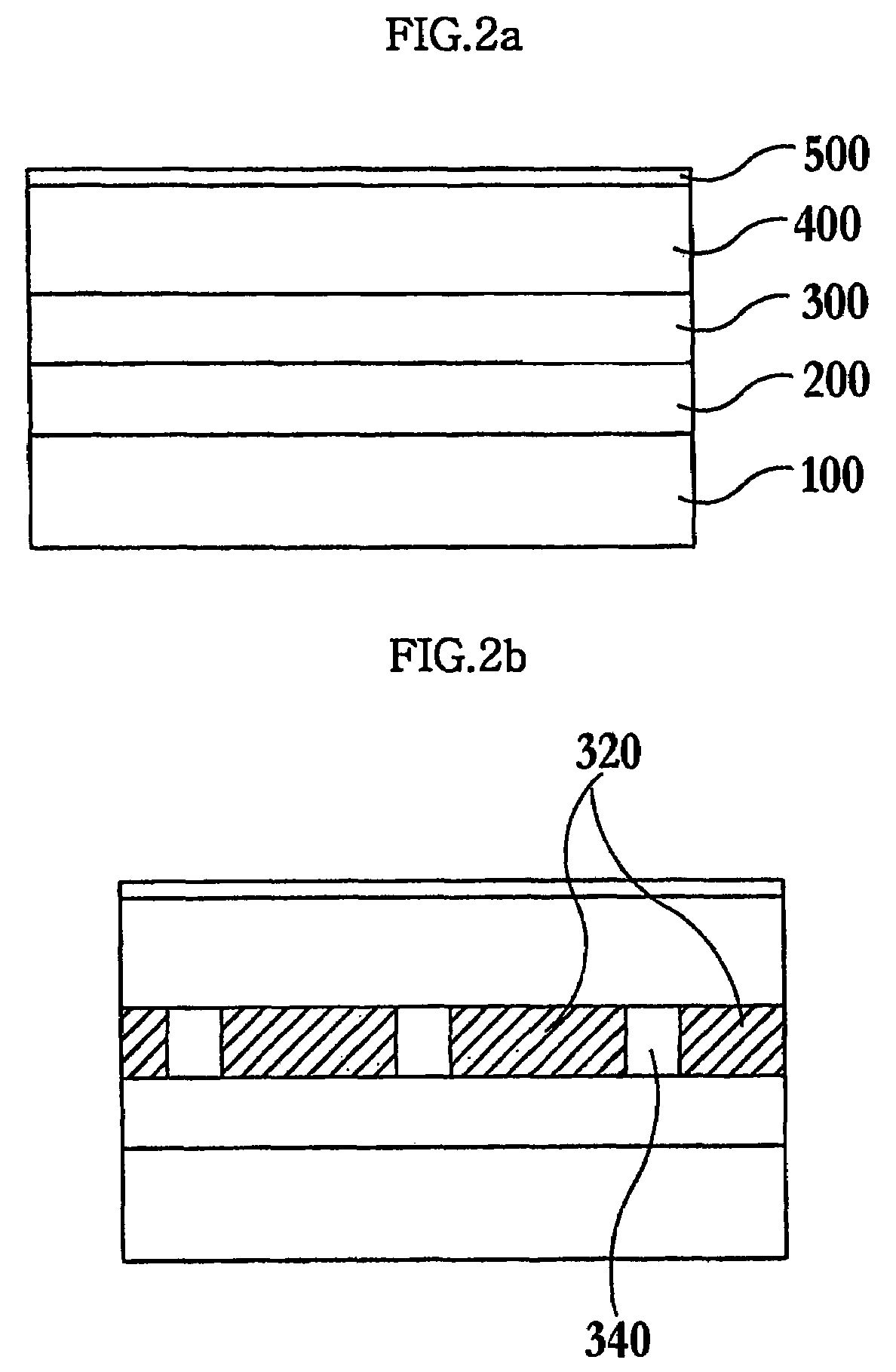
[0057]FIGS. 2a to 2d are schematic views illustrating a preferred embodiment of the present invention. The material that is thermally treated in the present invention comprises a dielectric substrate 100, a buffer layer 200 deposited on the dielectric substrate 100, an amorphous material 300 deposited on the buffer layer 200, a cap layer 400 formed on the amorphous material 300, and a metal 500 deposited on the cap layer 400 (see 2a).

[0058]The dielectric substrate 100 is not limited to a specific material. However, it is preferable that the dielectric material a material selected from glass, quartz, a single crystal wafer covered with an oxide film is used as the dielectric material in order to ensure the uniformity of the temperat...


PUM

PropertyMeasurementUnit
temperatureaaaaaaaaaa

Abstract

The present invention provides a phase transition method of an amorphous material, comprising steps of: depositing the amorphous material on a dielectric substrate; forming a cap layer on the amorphous material; depositing a metal on the cap layer; and crystallizing the amorphous material. According to the present invention, the surface of the amorphous material is protected by the cap layer, so that clean surface can be obtained and the roughness of the surface can be remarkably reduced during thermal process and sample handling. In addition, the cap layer is disposed between the amorphous material and the metal to diffuse the metal, so that the metal contamination due to the direct contact of the metal and the amorphous material in the conventional method can be remarkably reduced.

Description

[0001]This application is a National Stage application under 35 U.S.C. § 371 of and claims the benefit of International Application No. PCT / KR03 / 02362, filed on Nov. 6, 2003, published in the English language on May 21, 2004 as International Publication Number WO 2004 / 042805 A1, which claims priority to Korean Application No. 10-2002-0068994 filed on Nov. 8, 2002, all of which are hereby incorporated by reference.TECHNICAL FIELD[0002]The present invention relates to a phase transition method of an amorphous material, and more specifically, to a method phase transition method of an amorphous material capable of implementing a uniform thin film without any contact of a metal and the amorphous material.BACKGROUND ART[0003]A thin film transistor (TFT) is a switching device in which a polysilicon thin film is used as an active layer. In general, the thin film transistor is used as an active device of an active matrix liquid crystal display apparatus, a switching device of an electro-lumi...

Claims


Application Information

Patent Timeline
Patent Type & Authority Patents(United States)
IPC IPC(8): H01L21/20
CPCH01L21/0242H01L21/02422H01L21/02667H01L21/02532H01L21/268H01L21/02672H01L21/20
Inventor JANG, JINCHOI, JONGHYUNKIM, DO-YOUNGCHOO, BYOUNG-KWON
Owner SILICON DISPLAY TECH CO LTD
Why Eureka
Try Eureka