Nonvolatile memory element
a technology of transition metal oxide and memory element, which is applied in the field of nonvolatile memory, can solve the problems of inability to control the properties of change in the resistance of the element, the degree of change in the resistance is small, so as to achieve the effect of controlling the properties of change in the resistance and the switching properties, and improving the resistance and switching properties
- Summary
- Abstract
- Description
- Claims
- Application Information
AI Technical Summary
Benefits of technology
Problems solved by technology
Method used
Image
Examples
example 1
[0031]FIG. 3 is a cross sectional diagram showing the structure of a nonvolatile memory element according to Example 1 of the present invention, and the manufacturing method for the same is as follows.
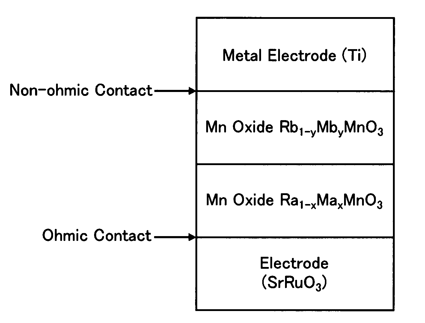
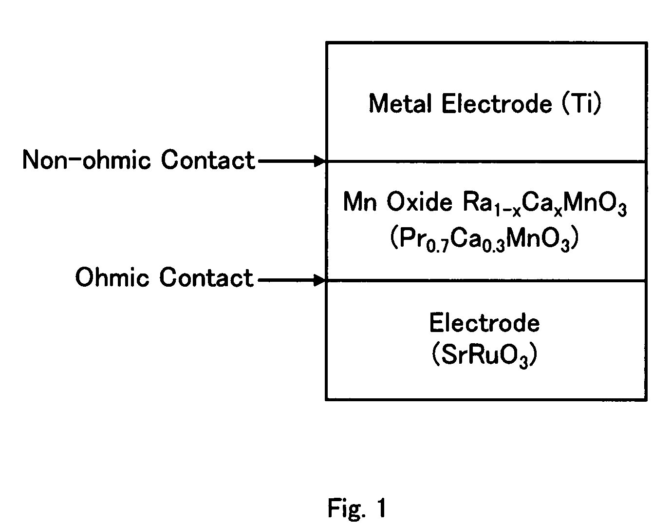
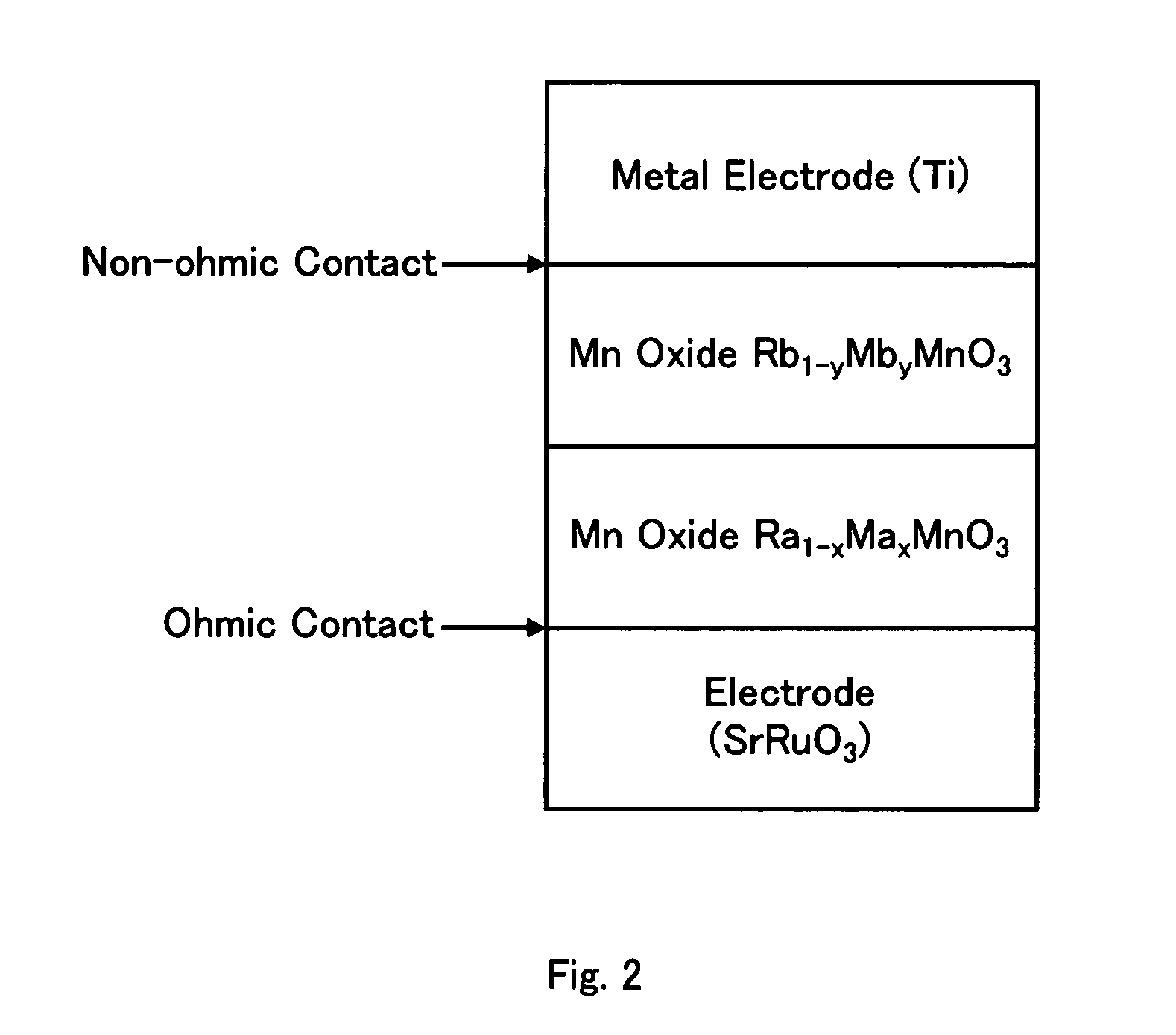
[0032]A conductor having a deep work function, such as SrRuO3, having a thickness of 80 nm, which became an ohmic electrode, was formed on an SrTiO3 oxide single crystal substrate, which is an insulator, through pulse laser deposition under such conditions for fabrication that the temperature of the substrate was 700° C. and the oxygen pressure was 100 mTorr, and subsequently, Pr0.7Ca0.3MnO3 having a thickness of 100 nm, which became a p type semiconductor, was formed under the same conditions for fabrication, and then, Sm0.7Ca0.3MnO3 having a bandwidth which is smaller than that of Pr0.7Ca0.3MnO3 and insulation which is higher than that of Pr0.7Ca0.3MnO3 and having a thickness of 2 nm was formed on top of this under the same conditions for fabrication, and after that, the temperature ...
example 2
[0042]FIG. 5 is a cross sectional diagram showing the structure of a nonvolatile memory element according to Example 2 of the present invention, and the manufacturing method for the same is as follows.
[0043]A conductor having a deep work function, such as SrRuO3, having a thickness of 80 nm, which became an ohmic electrode, was formed on an SrTiO3 oxide single crystal substrate, which is an insulator, through pulse laser deposition under such conditions for fabrication that the temperature of the substrate was 700° C. and the oxygen pressure was 100 mTorr, and subsequently, La0.7Sr0.3MnO3 having a thickness of 100 nm, which became a metallic perovskite-type transition metal oxide, was formed under the same conditions for fabrication, and then, Sm0.7Ca0.3MnO3 having a bandwidth which is smaller than that of La0.7Sr0.3MnO3 and insulation which is higher than that of La0.7Sr0.3MnO3 and having the same thickness as a layer of one molecule (0.4 nm) to five molecules (2 nm) was formed on ...
PUM
 Abstract
Description
Claims
Application Information
 - R&D
- Intellectual Property
- Life Sciences
- Materials
- Tech Scout
- Unparalleled Data Quality
- Higher Quality Content
- 60% Fewer Hallucinations
Browse by: Latest US Patents, China's latest patents, Technical Efficacy Thesaurus, Application Domain, Technology Topic, Popular Technical Reports.
© 2025 PatSnap. All rights reserved.Legal|Privacy policy|Modern Slavery Act Transparency Statement|Sitemap|About US| Contact US: help@patsnap.com


