Layout of power device

a power device and integrated circuit technology, applied in the direction of amplifiers with min 3 electrodes or 2 pn junctions, program control, instruments, etc., can solve the problems of affecting the performance of the power device, and affecting the performance of the remaining transistors, so as to reduce cross talk, reduce the effect of mismatch problems, and simple wiring layou

Active Publication Date: 2009-08-04
UNITED MICROELECTRONICS CORP
View PDF7 Cites 0 Cited by
  • Summary
  • Abstract
  • Description
  • Claims
  • Application Information

AI Technical Summary

Benefits of technology

[0008]Accordingly, the present invention is directed to a layout of a power device comprising a symmetrically balanced input signal path and a output signal path to reduce or eliminate the mismatch problems. The layout uses a simple wiring layout to reduce cross talk between metal interconnects. In addition, the layout in the present invention can be applied to a power device such as the singled-ended differential pair power device.
[0011]Because the power device with symmetrically balanced input signal path and output signal path has a simple wiring layout, the mismatch problems may be reduced or eliminated and also cross talk between metal interconnects is reduced. In addition, the layout of the present invention may be applied to a singled-ended, differential pair power device.

Problems solved by technology

In some particular applications (for example, high frequency operations), the internal layout of the power device often directly affects the performance.
For example, the non-symmetric connective relationships between transistors in the layout will often lead to mismatches.
Because the current output from the power amplifier is quite large, the current is often large enough to damage the mismatched transistor so that the remaining transistors must take up the total output current.
Because the power amplifier drives a heavy load, a portion of the remaining transistors may malfunction due to the overheating resulting from the rise in temperature.
When more and more transistors fail, the remaining transistors have to take up a heavier load.
Ultimately, a chain reaction may occur to shut down the entire power amplifier.
If the connectivity from each transistor to the next stage is too complicated, significant signal loss may result.
The foregoing H-shaped layout has difficulties applying to a differential circuit.
If the H-shaped layout is applied to a differential pair, cross talk between metal interconnects is a problem.

Method used


Image

  • Layout of power device
  • Layout of power device
  • Layout of power device

Examples


Embodiment Construction

[0021]Reference will now be made in detail to the present preferred embodiments of the invention, examples of which are illustrated in the accompanying drawings. Wherever possible, the same reference numbers are used in the drawings and the description to refer to the same or like parts.

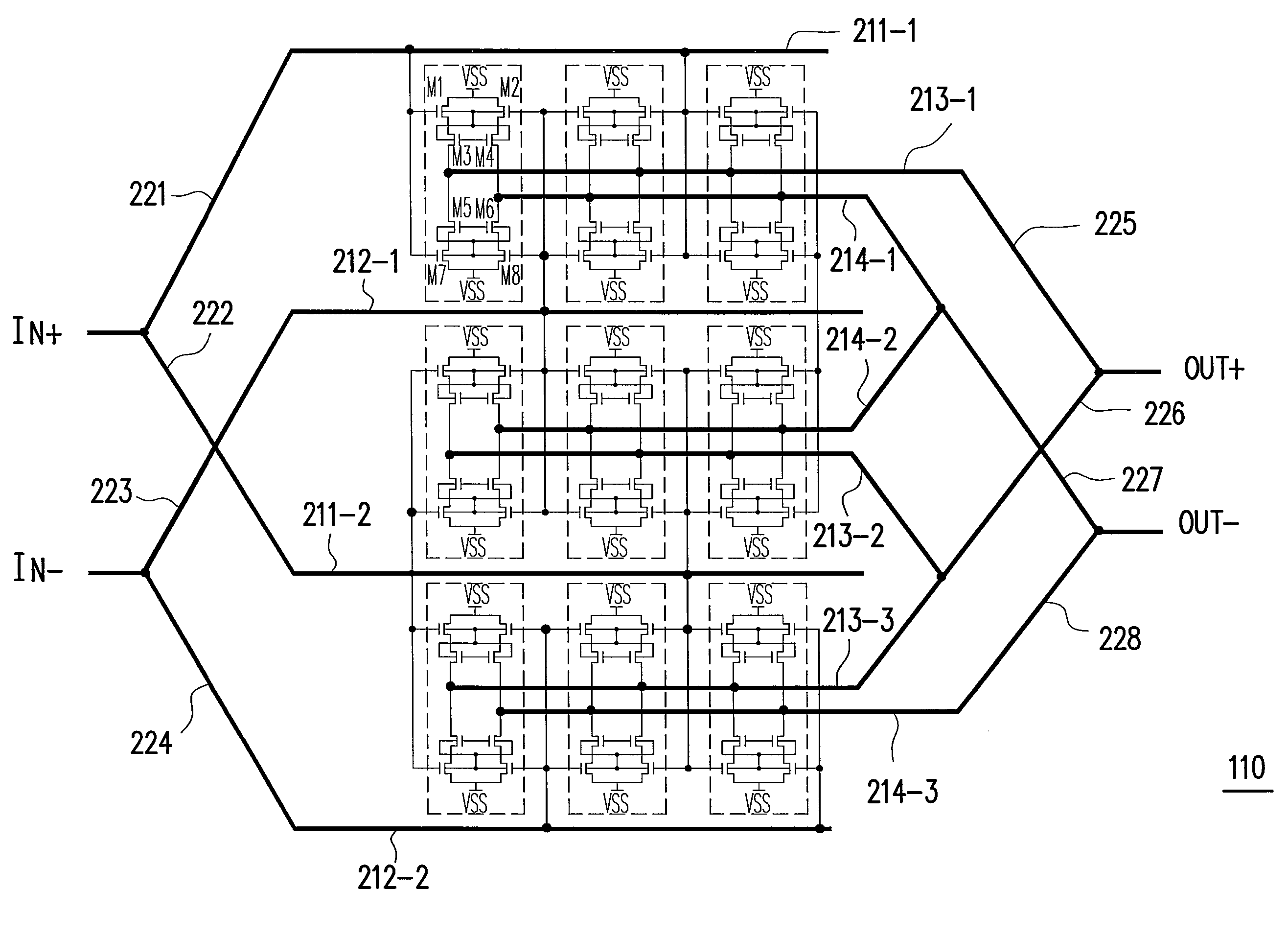
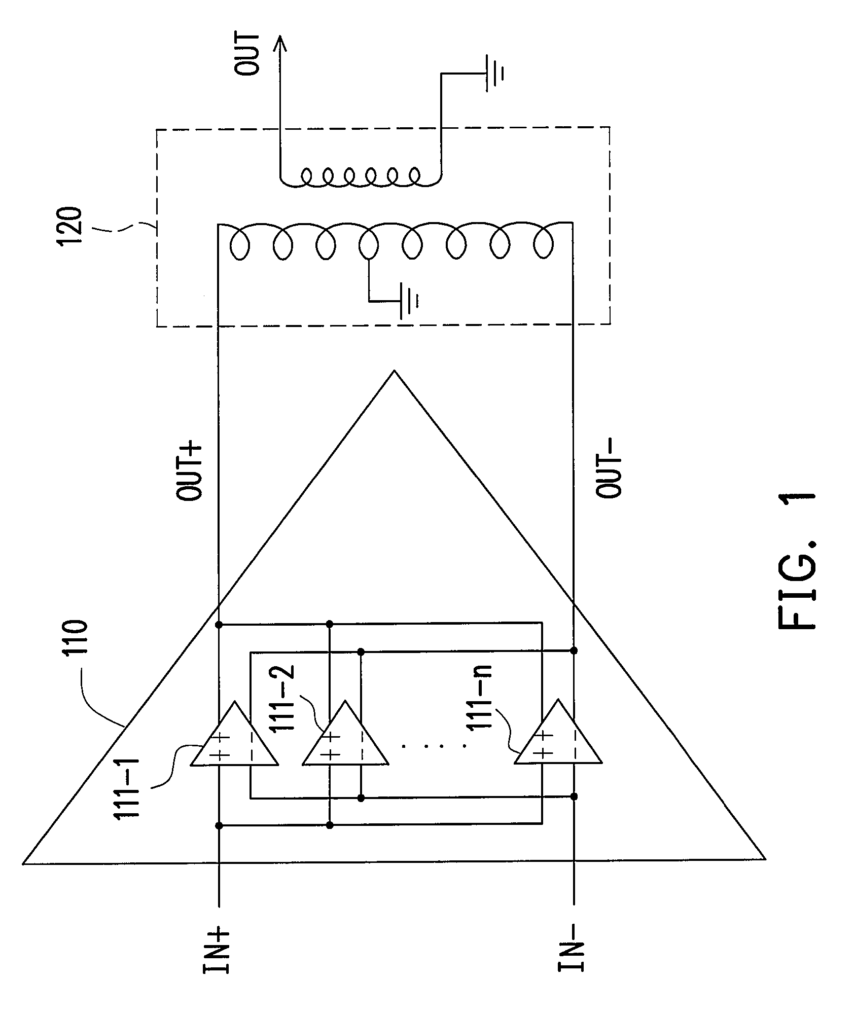
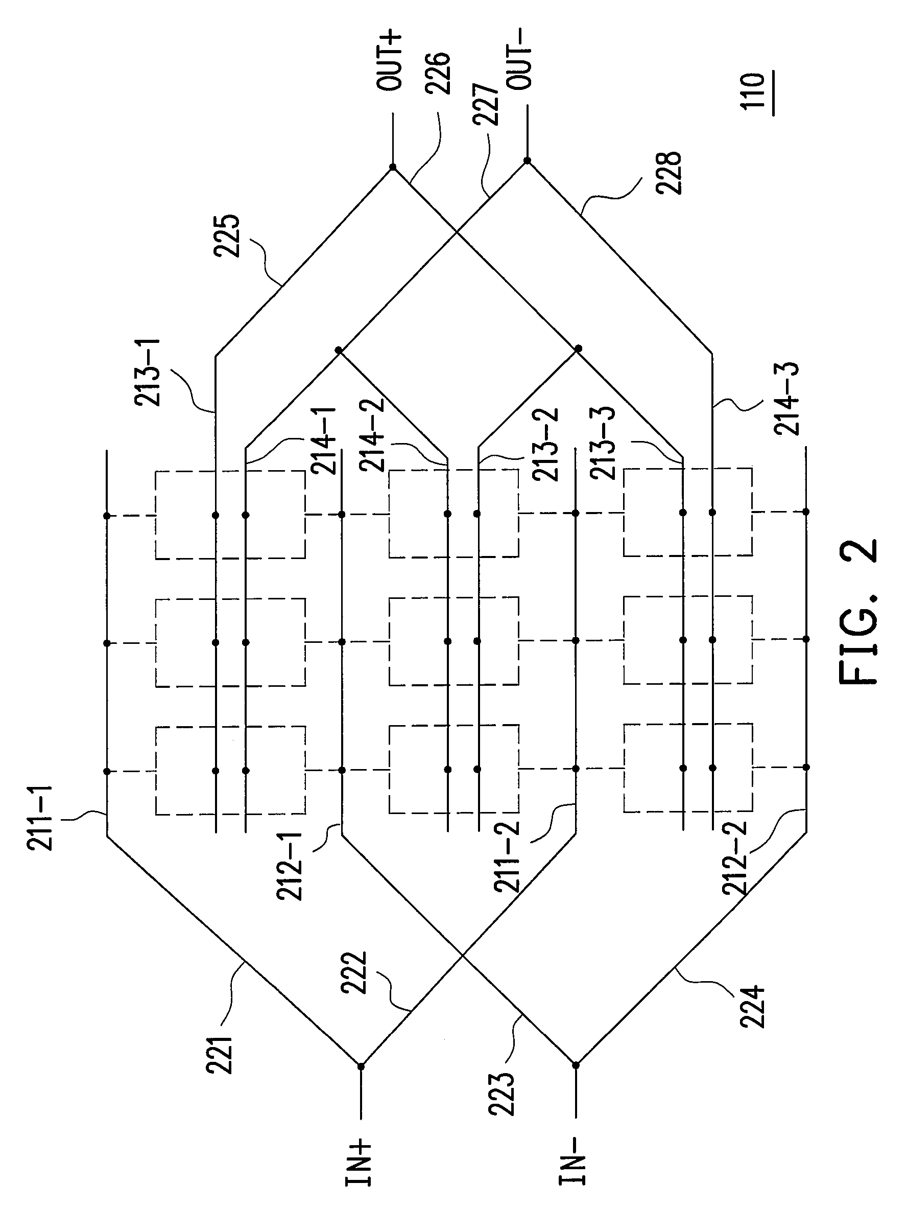
[0022]Power devices are mainly used to provide a large power-driving capability. Examples of power devices include buffer and power amplifier (PA). FIG. 1 is an application example of a power amplifier according to one embodiment of the present invention. Because differential signals have better noise rejection, most analog or radio frequency signals use a differential circuit. As shown in FIG. 1, the differential power amplifier 110 receives a differential signal pair through a first port (for example, the positive input port IN+) and a second port (for example, the negative input port IN−). After the differential signal pair is amplified, a large power differential signal pair is output through a t...


PUM


Abstract

A layout of a power device is provided. The layout includes a substrate, a unit array, a plurality of first, second, third and fourth signal paths, and a first, second, third and fourth port. The unit array with a plurality of rows is disposed on the substrate. Each row of the unit array includes a plurality of units. The first and second signal paths on the substrate are disposed on a first side and a second side of corresponding odd-numbered rows of the unit array. The third and the fourth signal paths on the substrate are disposed above a corresponding row of the unit array. The first to fourth ports on the substrate are electrically connected to the first to fourth signal paths respectively.

Description

BACKGROUND OF THE INVENTION[0001]1. Field of the Invention[0002]The present invention relates to a layout of an integrated circuit, and more particularly to a layout of a power device.[0003]2. Description of Related Art[0004]The power device (for example, a power amplifier) of an integrated circuit needs to have several groups of circuit units connected and output in parallel in order to satisfy the large power requirements of the next circuit stage. In some particular applications (for example, high frequency operations), the internal layout of the power device often directly affects the performance. For example, the non-symmetric connective relationships between transistors in the layout will often lead to mismatches. When micro-mismatch between the parallel-connected transistors of the power amplifier, one of the transistors may operate at a temperature environment higher than the other transistors. Since the operating current of a transistor is closely related to the temperature...

Claims


Application Information

Patent Timeline
Patent Type & Authority Patents(United States)
IPC IPC(8): G06F17/50H01L27/088H03F1/00
CPCH03F3/211H03F3/604H03F3/45475
Inventor AGHAHASSAN, HOUSHANGYEN, ALBERT KUO HUEIREED, CHUNG-CHEWU, TSUNG-CHIEN
Owner UNITED MICROELECTRONICS CORP
Why Eureka
Try Eureka