Filter device

a filter device and filter technology, applied in the field of filter devices, can solve the problems of increased chip area, degraded image quality, and limited filter length

Active Publication Date: 2009-08-04
LAPIS SEMICON CO LTD
View PDF6 Cites 10 Cited by
  • Summary
  • Abstract
  • Description
  • Claims
  • Application Information

AI Technical Summary

Benefits of technology

[0032]It is an object of the present invention to provide a filter device which is capable of solving the problems associated with the prior art, and precisely suppressing overshoot and undershoot in a relatively simple circuit configuration while limiting an increase in the chip area.
[0036]According to one aspect of the present invention, since the maximum value and minimum value to be used in the limiter circuit are detected in the output signals from the unit delay elements of the filter, overshoot and undershoot can be completely eliminated.
[0040]According to another aspect of the present invention, since output signals supplied to the maximum / minimum detector circuit from the unit delay elements may be sufficiently taken at three points, irrespective of the number of taps, overshoot and undershoot can be completely eliminated without requiring the complicated circuit configurations of the maximum / minimum detector circuit and the limiter circuit.

Problems solved by technology

However, when the filter 10 is mounted, for example, in a semiconductor integrated circuit, the filter length must be limited due to physical limitations.
Also, a luminance component can be mixed into a color component, giving rise to degraded image quality.
(a) The filter device of Japanese Patent Kokai No. 8-79558 includes the first and second LPFs for providing a single filtering effect and the mixer for controlling the mixing ratio, resulting in an increased chip area, and cannot completely eliminate the overshoot because the filter device basically involves a switch between the first and second LPFs.
(b) The filter device of Japanese Patent Kokai No. 2002-94358 includes the HPF, and replaces a boundary plane with another signal by the boundary signal generator, synthesis signal generator, and synthesizer to control the mixing ratio, resulting in an increased chip area. Moreover, while a filter is employed for removing a sub-carrier frequency component from a luminance signal, this filter is not necessary and rather adversely affects.
(c) Assuming that Japanese Patent Kokai No. 8-79558 and Japanese Patent Kokai No. 2002-94358 are applied for removing the overshoot 21 and undershoot 22 generated in the filter device of FIG. 2, measures must be taken, such as increasing the number of the filters 10, resulting in not only an increased chip area but also difficulties in removing the overshoot 21 and undershoot 22 without making the circuit configuration complicated.

Method used


Image

  • Filter device
  • Filter device
  • Filter device

Examples


Embodiment Construction

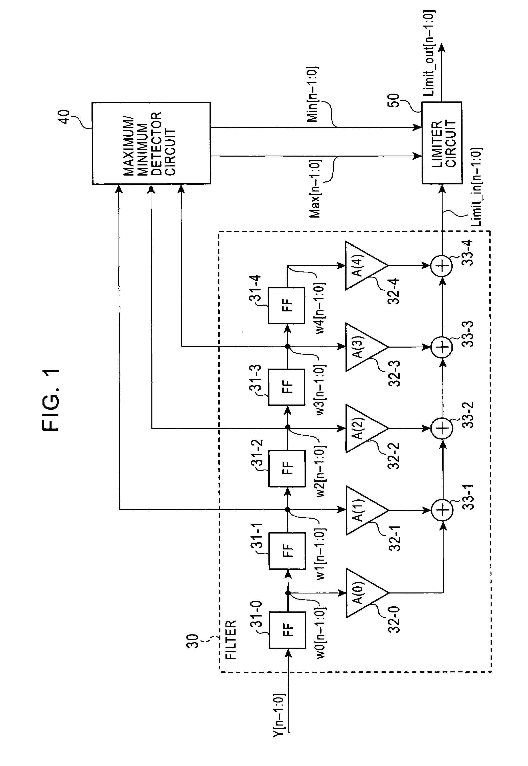
[0053]A filter device according to the present invention comprises a digital filter, a maximum / minimum detector circuit, and a limiter circuit.

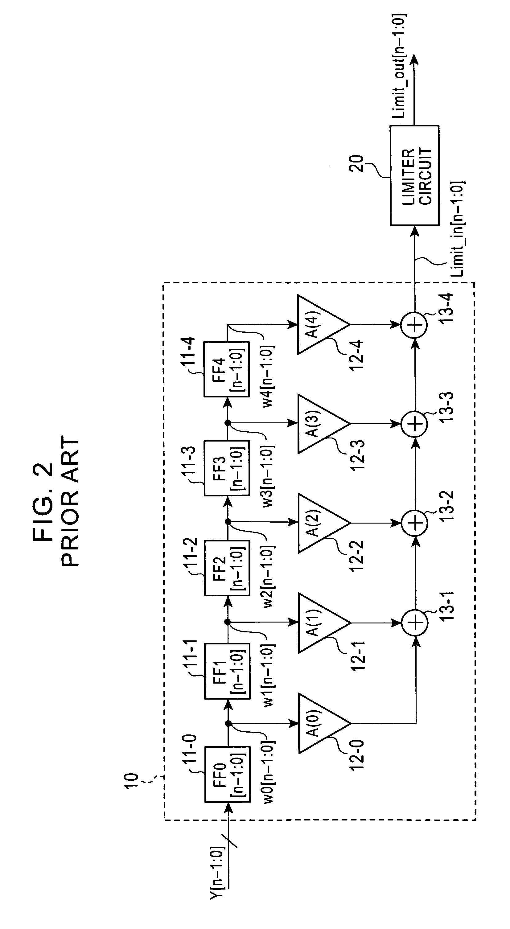
[0054]The digital filter includes unit delay elements (for example, FF) chained together and having (M+1) stages (where M is a positive integer equal to or more than two) and operable in response to an incoming (n+1) bit (where n is a positive integer) digital input signal, for shifting the digital input signal at the respective stages; (M+1) multipliers respectively connected to outputs of the unit delay elements at the respective stages for multiplying output signals of the unit delay elements at the respective stages by predetermined filter coefficients, respectively; and adder circuit chained together and having M stages and connected to the outputs of the (M+1) multiplier circuits for summing output signals of the respective multiplier circuits to supply a filtered output signal.

[0055]In overshoot and undershoot which can occur in the di...


PUM


Abstract

A filter device comprises a digital filter, a maximum / minimum detector circuit, and a limiter circuit. The digital filter includes unit delay elements chained together and having M stages (M is an integer equal to or larger than two) for shifting an n-bit (n is a positive integer) digital input signal; n multiplier circuits for multiplying output signals from the unit delay elements at the respective stages by predetermined filter coefficients, respectively; and adder circuits chained together and having (M−1) stages for summing output signals from the respective multiplier circuits to supply a filtered output signal. The maximum / minimum detector circuit detects a maximum value detection signal and a minimum value detection signal in the output signals supplied from the unit delay elements. The limiter circuit limits a minimum value of the filtered output signal based on the maximum value detection signal, and limits a minimum value of the filtered output signal based on the minimum value detection signal.

Description

BACKGROUND OF THE INVENTION[0001]1. Field of the Invention[0002]The present invention relates to a filter device capable of generating a filtered output signal free from overshoot and undershoot possibly occurring in an output of a low pass digital filter used for digital image signal processing and the like.[0003]2. Description of the Related Art[0004]Conventionally, there is known a lowpass filter device (for passing low frequency components therethrough) for filtering out high frequency components of a video signal, for example, in digital image signal processing.[0005]FIG. 2 is a schematic diagram of a conventional filter device for use in the digital image signal processing.[0006]This filter device comprises a low pass FIR (Finite Impulse Response) digital filter 10 having a filter length corresponding to, for example, five stages, and a limiter circuit 20 for limiting a maximum value and a minimum value of an output of the digital filter 10.[0007]The FIR digital filter 10 comp...

Claims


Application Information

Patent Timeline
Patent Type & Authority Patents(United States)
IPC IPC(8): H04N5/00H03H17/02H03H17/06H04N5/20H04N5/217
CPCH03H17/0219H03H17/06G06T5/20G06T5/002G06T2200/28H04N5/14
Inventor IHA, YASUSHIAKIYAMA, TAKAAKI
Owner LAPIS SEMICON CO LTD
Why Eureka
Try Eureka