Multilayer capacitor, manufacturing method thereof
a manufacturing method and capacitor technology, applied in the field of multi-layer capacitors, can solve the problems of increasing the difficulty of reducing the esl, the difficulty of keeping the fluctuation of the power source voltage within tolerances, and the need to further reduce the esl, so as to reduce the esl and the manufacturing method of the capacitor. , the effect of low manufacturing cos
- Summary
- Abstract
- Description
- Claims
- Application Information
AI Technical Summary
Benefits of technology
Problems solved by technology
Method used
Image
Examples
first embodiment
(Multilayer Capacitor)
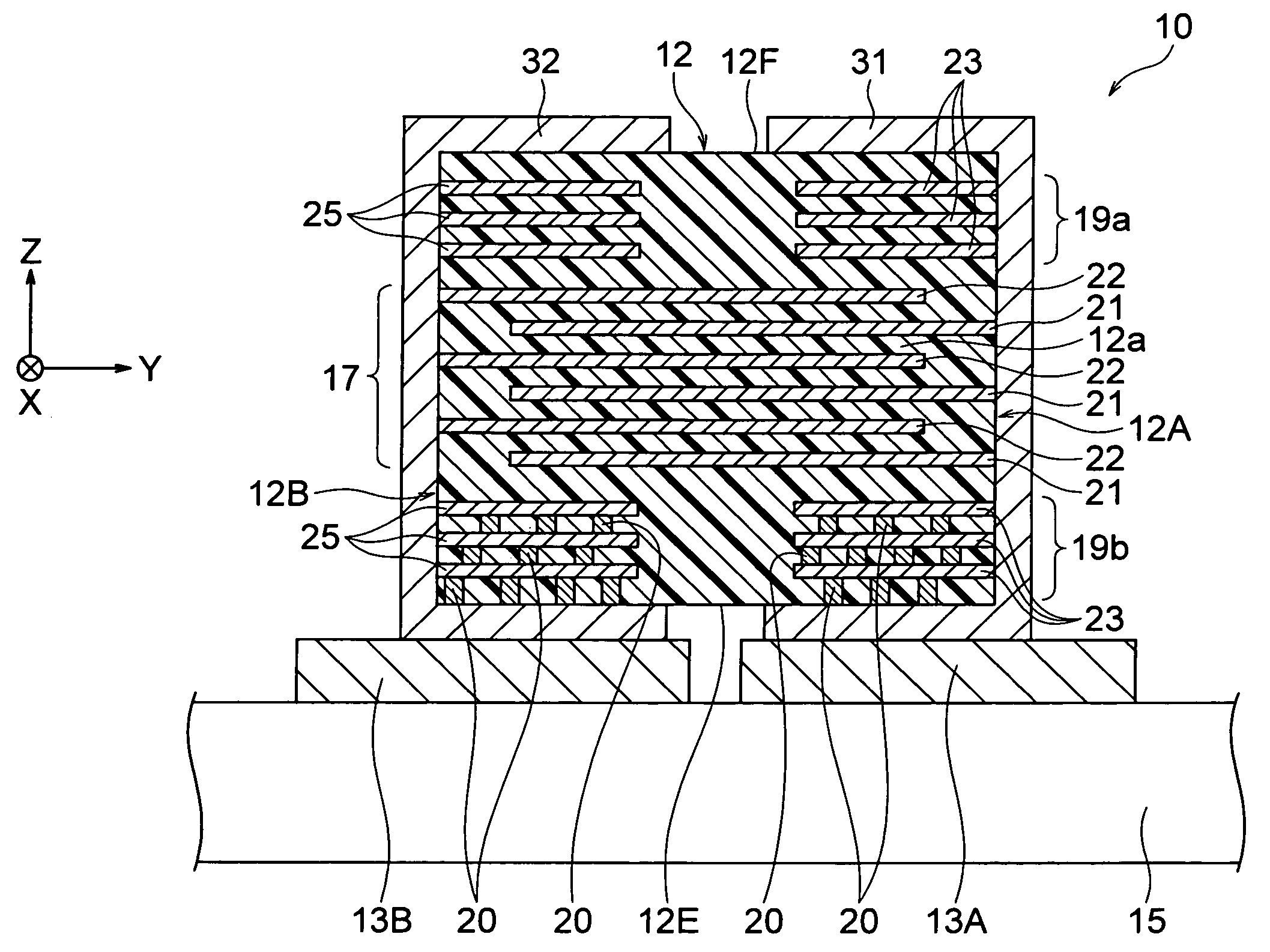
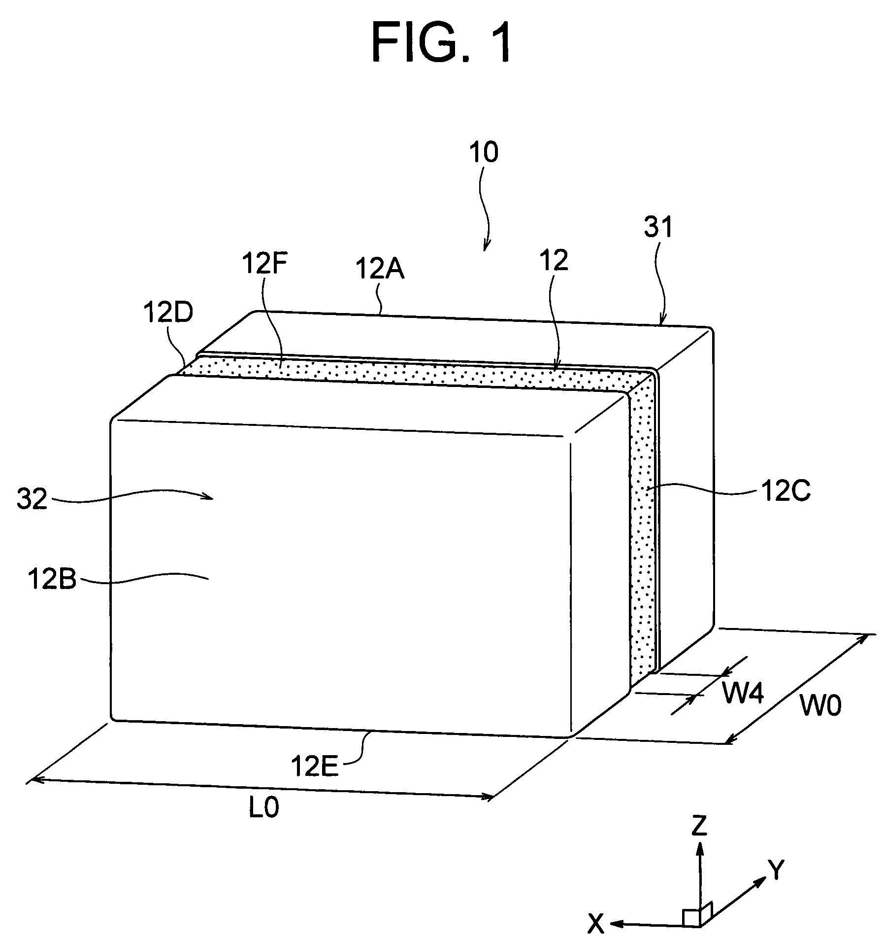
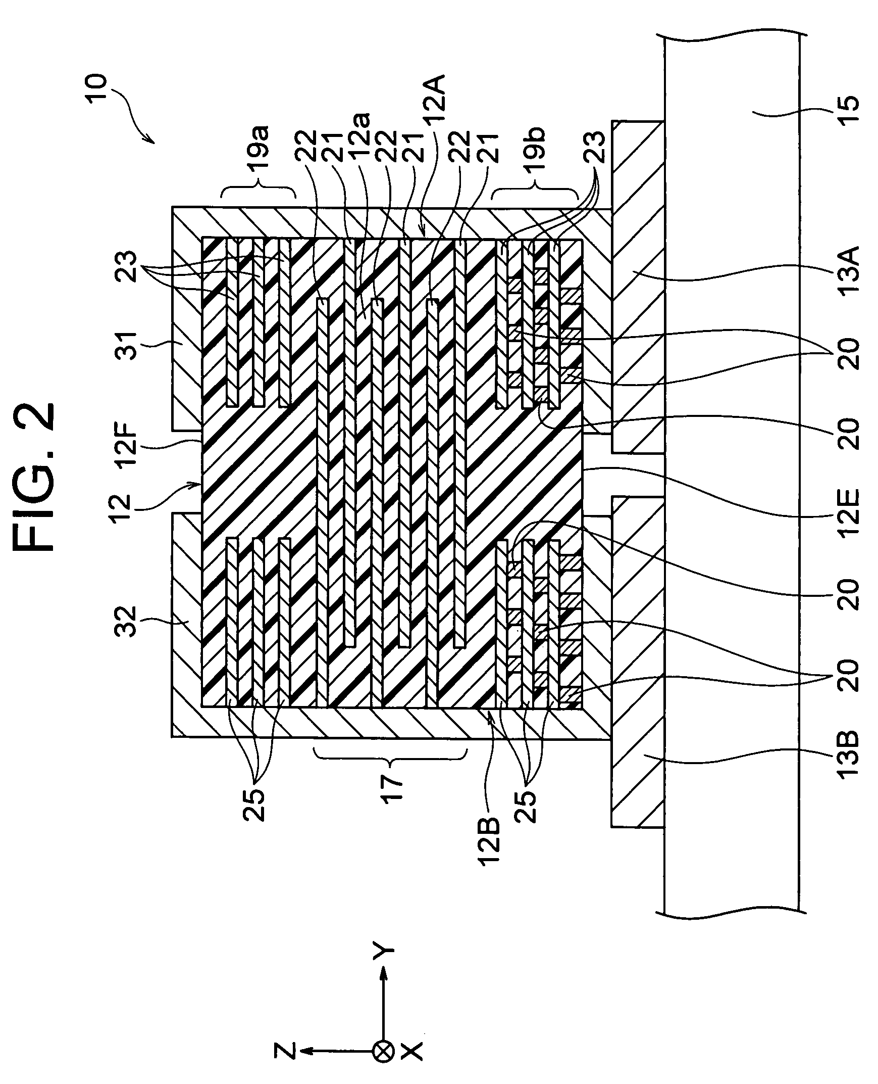
[0081]Whole constitution of a multilayer ceramic capacitor (herein after simply referred to as a “multilayer capacitor) 10 of a first embodiment of the present invention is specified. As shown in FIG. 1, the multilayer capacitor 10 comprises a dielectric body 12, a rectangular parallelepiped shaped sintered body obtained by firing a stack of a plurality of ceramic green sheets as dielectric layers.
[0082]The dielectric body 12 comprises a first side face 12A and a second side face 12B opposed to the first side face. Also, the dielectric body 12 comprises a third side face 12C and a fourth side face 12D adjacent to the first side face 12A and the second side face 12B, parallel to stacking direction Z of the dielectric layer and opposed each other.
[0083]In the present embodiment, preferably, as shown in FIG. 1, width L0 of the first side face 12A and the second side face 12B in vertical direction to stacking direction Z (X-direction) of the dielectric layer is lar...
second embodiment
[0180]Next, a second embodiment of the present invention will be explained. Note that, in the following, explanation of matters common in the first embodiment and the second embodiment are omitted, and only different points of both embodiments will be explained.
[0181]As shown in FIG. 6A, in the present embodiment, in the first lead portion of the first internal conductor layer 21, the first space pattern 41 which is not connected to the first terminal electrode 31 is formed at a center position along with the first longitudinal direction side face 12A. Consequently, the first lead portion comprises a pair of branch lead patterns 21b led out from a main body 21a of the first internal conductor layer 21 to two corner portions wherein the first longitudinal direction side face 12A and the lateral side faces 12C and 12D of the dielectric body 12 are crossing.
[0182]When the width of the lateral direction Y of the dielectric body 12 is W0, the width W1 of the lateral direction Y of the br...
third embodiment
[0196]Next, a third embodiment of the present invention will be explained based on FIG. 7A to FIG. 7D. Note that, in the following, matters common in the first, the second and the third embodiments are omitted, and only different points of the above embodiments and the third embodiment will be explained.
[0197]In the present embodiment, other than substituting the second internal conductor layer 22 of the second embodiment with two types of the second internal conductor layers 322 shown in FIG. 7B and FIG. 7D and the second internal conductor layers 323 shown in FIG. 7D, a multilayer capacitor is composed in the same way as in the first embodiment.
[0198]In the present embodiment, the second internal conductor layer 322 shown in FIG. 7B is stacked via the dielectric layer 12a under the first internal conductor layer 21 shown in FIG. 7A which is the same as that of the second embodiment, and the first conductor layer 21 shown in FIG. 7C which is the same as the second embodiment is sta...
PUM
| Property | Measurement | Unit |
|---|---|---|
| diameter | aaaaa | aaaaa |
| pin hole diameter | aaaaa | aaaaa |
| hole diameter | aaaaa | aaaaa |
Abstract
Description
Claims
Application Information
 - R&D
- Intellectual Property
- Life Sciences
- Materials
- Tech Scout
- Unparalleled Data Quality
- Higher Quality Content
- 60% Fewer Hallucinations
Browse by: Latest US Patents, China's latest patents, Technical Efficacy Thesaurus, Application Domain, Technology Topic, Popular Technical Reports.
© 2025 PatSnap. All rights reserved.Legal|Privacy policy|Modern Slavery Act Transparency Statement|Sitemap|About US| Contact US: help@patsnap.com


