
Integrated modulator/laser assembly and a method of producing same

a technology of integrated modulators and laser assemblies, which is applied in the direction of optical elements, semiconductor lasers, instruments, etc., can solve the problems of low fabrication yield and limit the propagation span of ea-dfb assemblies of the type shown in fig. 1, and increase the frequency chirp

Inactive Publication Date: 2009-06-16
AVAGO TECHNOLOGIED FIBER IP SINGAPORE PTE LTD
View PDF16 Cites 0 Cited by
  • Summary
  • Abstract
  • Description
  • Claims
  • Application Information

AI Technical Summary

Benefits of technology

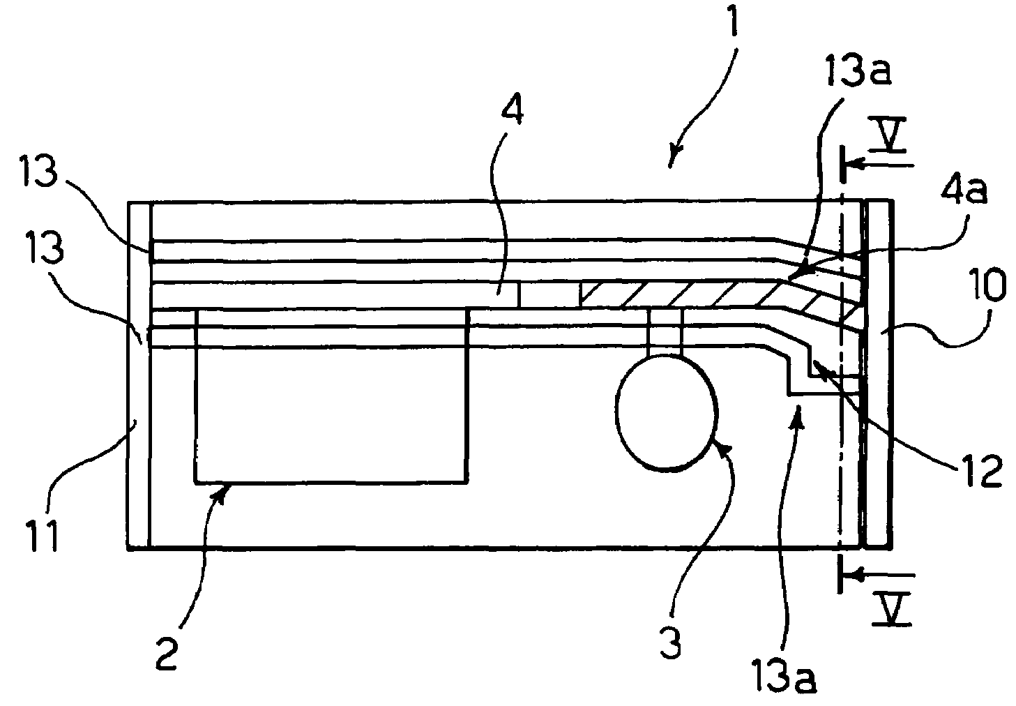
[0017]A preferred embodiment of the invention is an assembly including a laser source, such as a distributed feedback laser (DFB), integrated with a modulator, such as an electro-absorption modulator (EAM), having a common waveguide. The waveguide in the EAM section (EAM waveguide) has a distal end, which is bent and defines an inner side of the bent waveguide. A low reflectivity facet is arranged at the distal end of the EAM section. A mirror is arranged at the inner side of the distal end of the EAM waveguide to prevent any back reflection into the EAM waveguide from the low reflectivity facet and the two lateral trenches typically associated therewith: these two trenches extending at the sides of the common waveguide, and have respective bent distal ends extending at the sides of the bent distal end of the common waveguide. The mirror is preferably provided as a step formed in the trench arranged at the inner side of the distal end of the waveguide.

Problems solved by technology

Within these possible contexts of use, frequency chirp due to back-reflection from the modulator facet severely limits the propagation span at 10 Gb / s.
Minimizing the modulator facet reflection is thus a key issue in increasing the propagation span.
This requirement is very close or beyond the technical limits of most film deposition kits currently available, which leads to a low fabrication yield for EA-DFB assemblies of the type shown in FIG. 1.
This again undesirably increases the frequency chirp.

Method used


Image

  • Integrated modulator/laser assembly and a method of producing same
  • Integrated modulator/laser assembly and a method of producing same
  • Integrated modulator/laser assembly and a method of producing same

Examples


Embodiment Construction

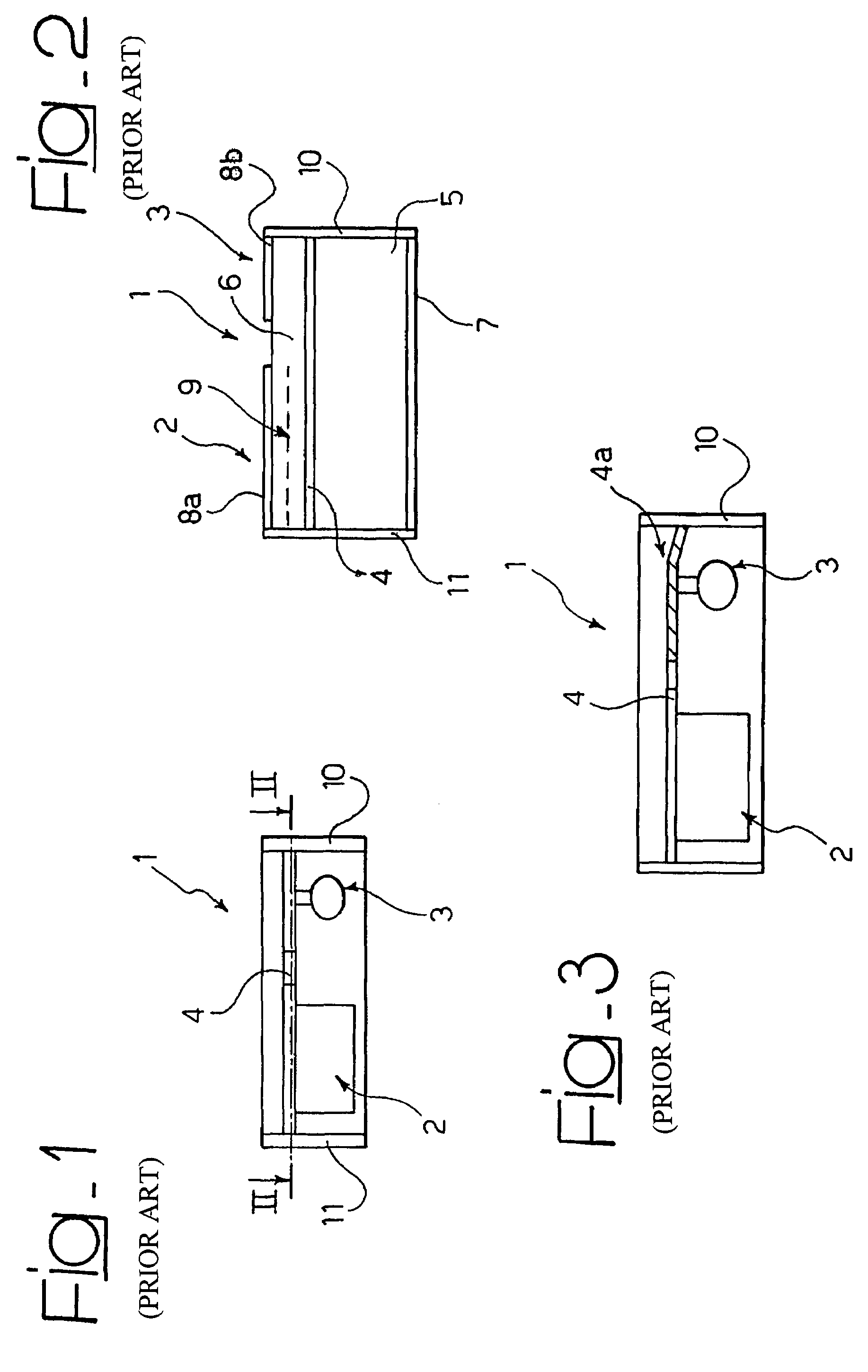
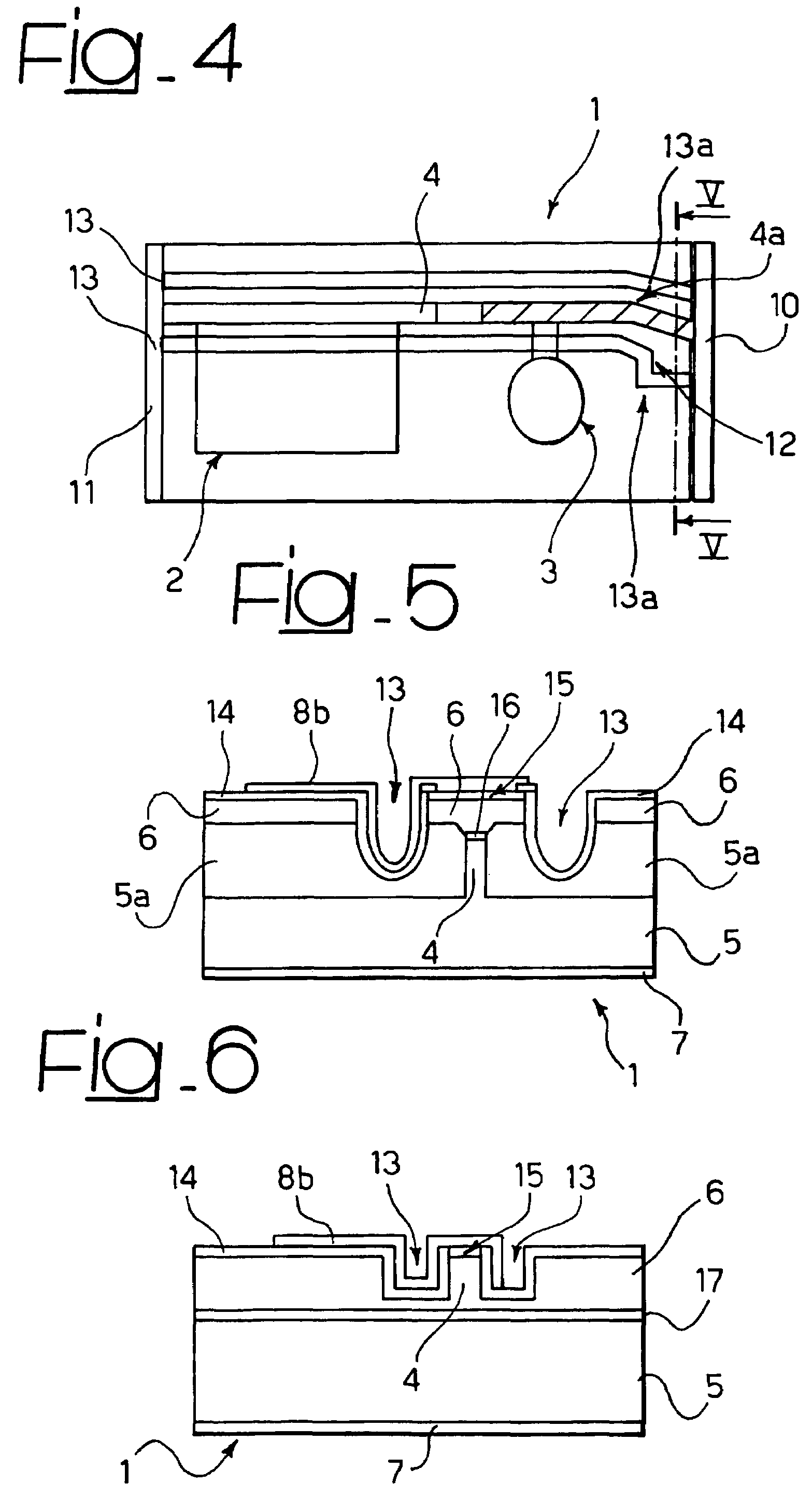
[0024]Throughout FIGS. 4 to 8, the same reference numerals introduced in FIGS. 1 to 3 have been used to designate parts / elements that are identical or equivalent to those already described in connection with FIGS. 1 to 3. Therefore, such parts / elements will not be described again in connection with FIGS. 4 to 8. Additionally, some parts or elements that are not essential for understanding and / or reproducing the invention have been omitted from some of FIGS. 4 to 8.

[0025]Essentially, in the arrangement shown in FIGS. 4 to 6, the bent-waveguide arrangement in the modulator section 3 of the EA-DFB assembly includes a micro mirror 12. The mirror 12 provides a low back-coupled reflection level while allowing (bent) trenches to be provided at the sides of the waveguide 4.

[0026]As explained, the bent-waveguide arrangement relaxes the requirements for the low reflectivity coating of the facet 10. The trenches provide a low capacitance with a narrow mesa structure. Finally, the micro mirror ...


PUM


Abstract

An laser/modulator assembly includes a laser source, such as a distributed feedback (DFB) laser, and a modulator, such as an electro-absorption modulator (EAM), integrated along a common waveguide. The waveguide has a distal end bent to define an inner side of the bent waveguide. A low reflectivity facet is arranged at the distal end of the waveguide, and a mirror is arranged at the inner side of the distal end of the waveguide to prevent any back reflection into the EAM waveguide from said low reflectivity facet, and the lateral trenches typically associated therewith.

Description

CROSS-REFERENCE TO RELATED APPLICATION[0001]This application claims the benefit of the priority of Great Britain Patent Application No. 0422311.1 filed on Oct. 8, 2004, which is hereby incorporated by reference in its entirety.[0002]1. Field of the Invention[0003]The present invention relates to integrated modulator / laser assemblies, such as e.g. those assemblies including an electro-absorption modulator (EAM) integrated with a distributed feedback laser (DFB).[0004]2. Discussion of the Background Art[0005]Assemblies including a low-chirp 1550 nm electro-absorption modulator integrated with a distributed feedback laser (EA-DFB) have been considered for use in 10-40 km fiber optic links for 10 Gb Ethernet and 40-80 km OC192 applications.[0006]Within these possible contexts of use, frequency chirp due to back-reflection from the modulator facet severely limits the propagation span at 10 Gb / s. Minimizing the modulator facet reflection is thus a key issue in increasing the propagation s...

Claims


Application Information

Patent Timeline
Patent Type & Authority Patents(United States)
IPC IPC(8): H01S3/08H01S3/113G02B6/12H01S5/026H01S5/028H01S5/12H01S5/22H01S5/227
CPCG02B6/12004H01S5/0265H01S5/1082H01S5/227H01S5/028H01S5/101H01S5/12H01S5/2214
Inventor CORIASSO, CLAUDIOFANG, RUI YUROGGERO, GUIDOROSSO, MARZIACODATO, SIMONE
Owner AVAGO TECHNOLOGIED FIBER IP SINGAPORE PTE LTD
Learn More