
Decision feedback equalization input buffer

a technology of input buffer and input input, which is applied in the direction of pulse manipulation, transmission monitoring, pulse technique, etc., can solve the problems of inter-symbol interference, timing errors and voltage errors, and channel bandwidth limitations

Active Publication Date: 2009-06-02
SAMSUNG ELECTRONICS CO LTD
View PDF9 Cites 18 Cited by
  • Summary
  • Abstract
  • Description
  • Claims
  • Application Information

AI Technical Summary

Benefits of technology

The solution enables reliable signal compensation and higher inter-circuit transfer rates by dynamically adjusting the equalization coefficient to accommodate varying errors, improving signal reliability and transfer efficiency.

Problems solved by technology

Communication between integrated circuit systems inevitably results in the generation of timing errors and voltage errors that occur in the inter-chip transmitted signals.
The common source of such errors is inter-symbol interference (ISI), which is caused by limitations in the channel bandwidth.
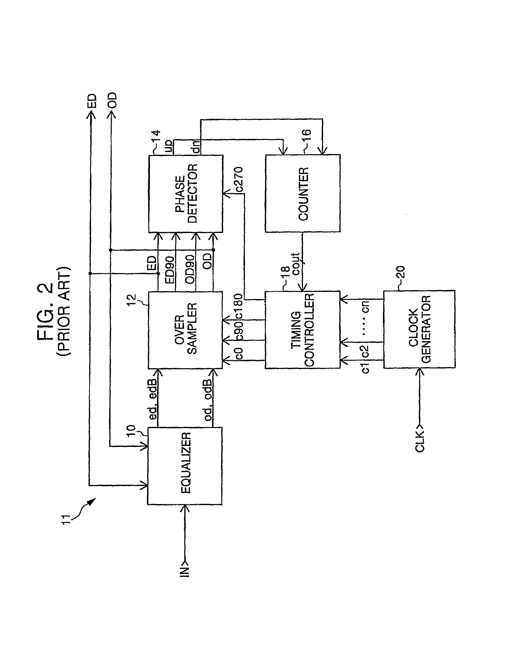
However, conventional DFE input buffers cannot efficiently compensate for timing and voltage errors caused by ISI, since the equalization coefficients in such buffers are fixed.
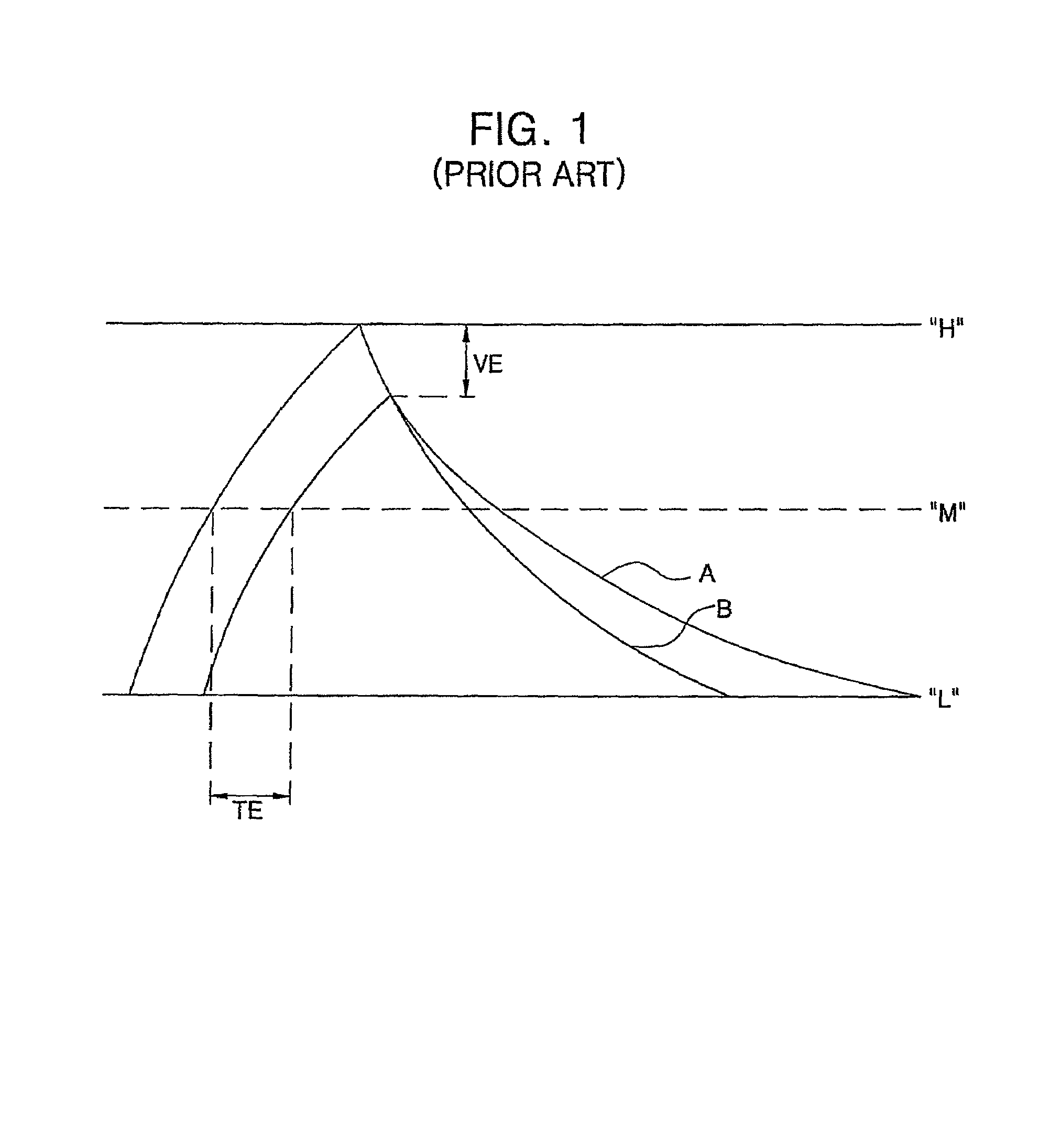
It can be seen that the erroneous input signal A experiences a timing error TE in the form of a timing delay, and a voltage error VE in the form of a reduced input voltage.
For this reason, the conventional equalizer circuit is incapable of accurately compensating for timing errors or voltage errors in the input signal over a range of operating conditions.

Method used


Image

  • Decision feedback equalization input buffer
  • Decision feedback equalization input buffer
  • Decision feedback equalization input buffer

Examples


Embodiment Construction

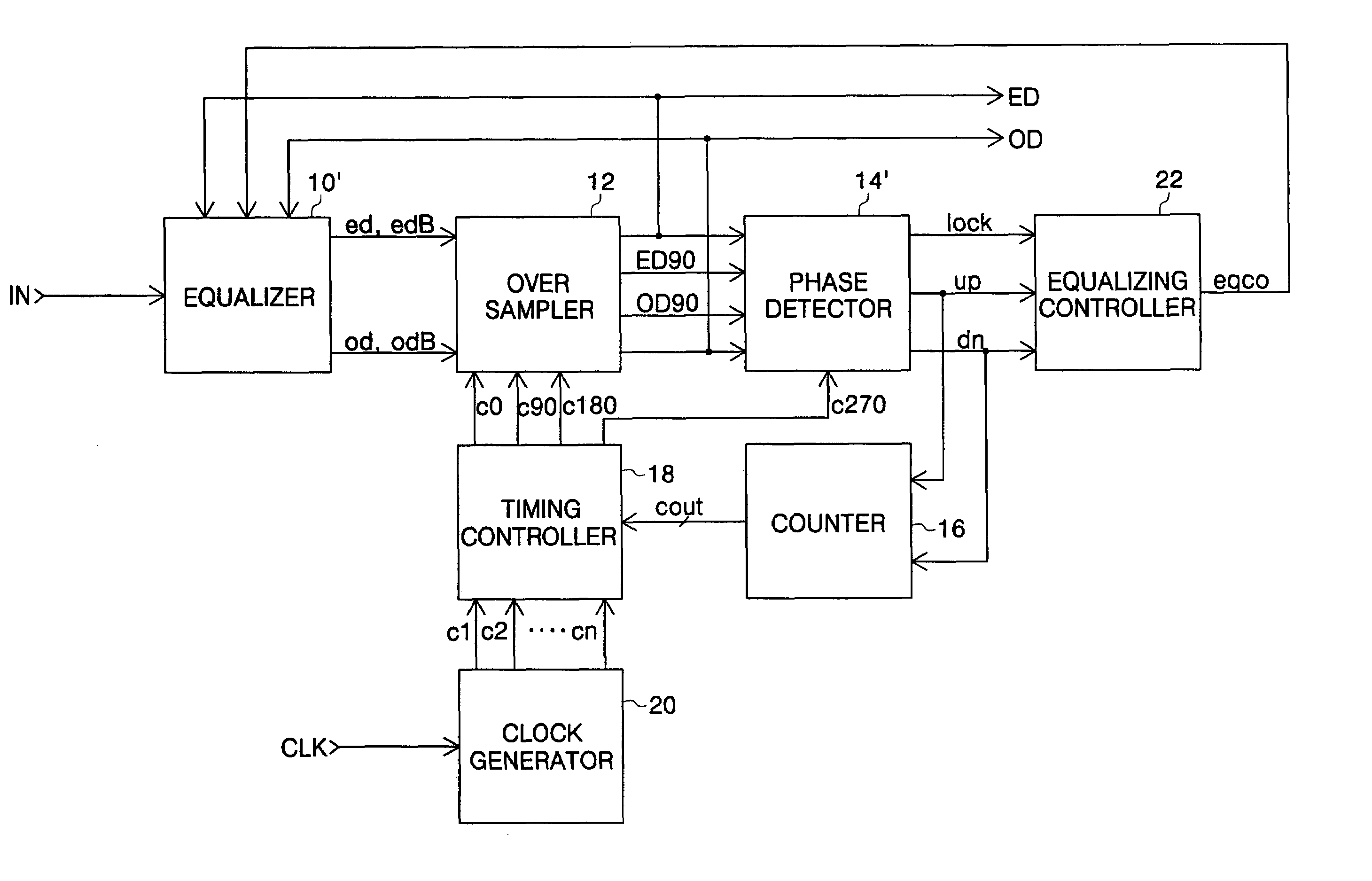
[0051]FIG. 4 is a block diagram of a DFE input buffer in accordance with the present invention. In the embodiment of FIG. 4, an equalizer 10′ amplifies the difference between an input signal IN including an ISI component, and an odd oversampled output signal OD (or ODB) multiplied by a variable equalization coefficient value β that is determined in response to a received value of an equalizing coefficient control signal eqco, to compensate for the ISI component. As a result, a first even amplified output signal ed, edB is generated. At the same time, the equalizer 10′ amplifies the difference between the input signal IN including the ISI component, and an even oversampled output signal ED (or EDB) multiplied by the variable equalization coefficient value β to compensate for the ISI component. As a result, a first odd amplified output signal od, odB is generated. The equalizer 10′ thus includes a circuit that generates the even amplified output signals ed / edB and a circuit that gener...


PUM


Abstract

In a decision feedback equalization (DFE) input buffer, timing and voltage errors, such as those caused by inter-symbol interference (ISI), are fully compensated. A variable equalizing coefficient is applied that accommodates, and compensates for, a range of timing errors TE or voltage errors VE that may be generated over a range of operating conditions. In this manner, accurate compensation is achieved, allowing for greater signal reliability and higher inter-circuit transfer rates. A decision feedback equalization (DFE) input buffer includes an equalizer that amplifies a difference in voltage level between an input signal and an oversampled signal in response to a variable equalizing control signal, the equalizer generating an amplified output signal. A sampling unit samples the amplified output signal in response to a sampling clock signal to generate the oversampled signal. A phase detector generates a timing control signal for controlling the timing of the activation of the sampling clock signal in response to a phase of the oversampled signal. An equalizing controller modifies the variable equalizing control signal in response to the timing control signal.

Description

RELATED APPLICATIONS[0001]This application claims the benefit of Korean Patent Application No. 2004-37966, filed on May 27, 2004, the disclosure of which is hereby incorporated herein by reference in its entirety.BACKGROUND OF THE INVENTION[0002]Communication between integrated circuit systems inevitably results in the generation of timing errors and voltage errors that occur in the inter-chip transmitted signals. The common source of such errors is inter-symbol interference (ISI), which is caused by limitations in the channel bandwidth. To accomplish high-speed inter-chip communication, the effect of ISI should be minimized.[0003]Decision feedback equalizer (DFE) input buffers are employed in contemporary systems to mitigate the harmful effects of ISI. However, conventional DFE input buffers cannot efficiently compensate for timing and voltage errors caused by ISI, since the equalization coefficients in such buffers are fixed.[0004]FIG. 1 is a waveform diagram illustrating the effe...

Claims


Application Information

Patent Timeline
Patent Type & Authority Patents(United States)
IPC IPC(8): H04B3/46H03H7/30H03H7/40H03K5/159H04B17/00H04Q1/20H03L7/00H03L7/081
CPCH03L7/0814H04L7/0331H04L25/03057H04L7/0087H03L7/0807H03L7/00
Inventor SOHN, YOUNG-SOO
Owner SAMSUNG ELECTRONICS CO LTD
Learn More