
Semiconductor apparatus

a semiconductor and apparatus technology, applied in the field of semiconductor apparatuses, can solve the problems of reducing the withstand-ability against voltage, complication of wiring process, and semiconductor apparatuses in the above-reference documents, and achieve the effects of preventing leakage current, high withstand voltage separating region, and easy modification of design

Active Publication Date: 2009-05-26
TOYOTA JIDOSHA KK
View PDF10 Cites 5 Cited by
  • Summary
  • Abstract
  • Description
  • Claims
  • Application Information

AI Technical Summary

Benefits of technology

The present invention provides a semiconductor apparatus with a low potential reference circuit region and a high potential reference circuit region between which signals are transmitted. The apparatus includes relay semiconductor devices for transmitting signals between the two regions. The apparatus also includes an insulating partition between the two regions, which prevents punch-through and leak current between the relay semiconductor devices and the circuit region. The insulating partition is filled with insulating material in a trench. The invention also provides a semiconductor apparatus with a high withstand voltage terminal region and a relay semiconductor device region for transmitting signals between the two regions. The invention also provides a semiconductor apparatus with a semiconductor substrate and an insulating film formed on the substrate. The technical effects of the invention include preventing punch-through and leak current, and achieving constant potential distribution.

Problems solved by technology

As a result, withstand-ability against voltage lowers due to drain wirings.
However, in case of a semiconductor apparatus of which potential difference between a high potential reference circuit region and a low potential reference circuit region exceeds 600V, it leads complication of wiring process due to thickened interlayer dielectric, cost-up, and the like.
However, semiconductor apparatuses in the above-reference documents have had following problems.
However, bending the high withstand voltage separating region leads to increase of chip area, which is obstacle to miniaturization of a substrate, as entirety.
Furthermore, since it is impossible to completely insulate the N drain layer of the high withstand NMOS and the N type layer in the high potential reference circuit region, leak current is inevitable.
Therefore, excessive power consumption occurs.
However, in case distance between the two N type layers is too short, punch-through breakdown occurs between N drain layer of the high withstand voltage NMOS and N type layer in the high potential reference circuit region.
Therefore, the trade-off relation is not always satisfied depending on required specification voltage and specification voltage restricts the trade-off balance.
Accordingly, the LOCOS method is not applicable to high withstand voltage type devices.
However, with this method, thickening the insulating region is not sufficient for enhancing voltage withstand-ability between drain wiring and the semiconductor layer, and width of the insulating layer must be taken wide to some extent.
In this connection, in case a wide trench exceeding 2 μm is formed, it is difficult to fill the trench with oxide film or poly crystal silicon film inside, which lacks feasibility.
Therefore, potential distribution gets uneven at the border portion of the semiconductor region and the insulating region and electric field is likely to concentrate at the border.

Method used


Image

  • Semiconductor apparatus
  • Semiconductor apparatus
  • Semiconductor apparatus

Examples


first exemplary embodiment

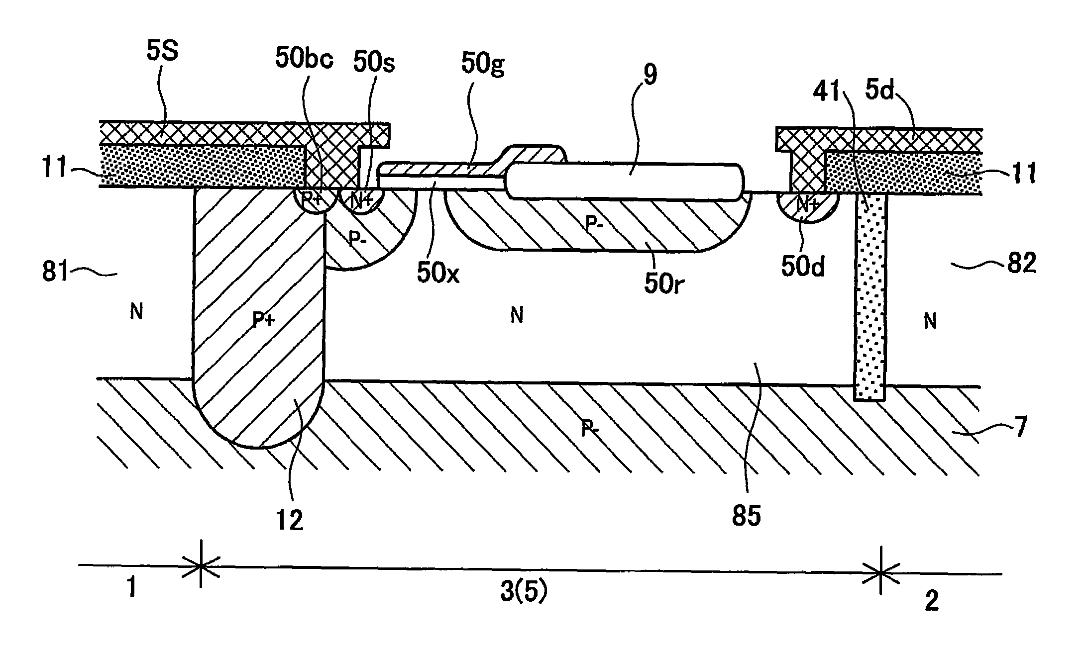
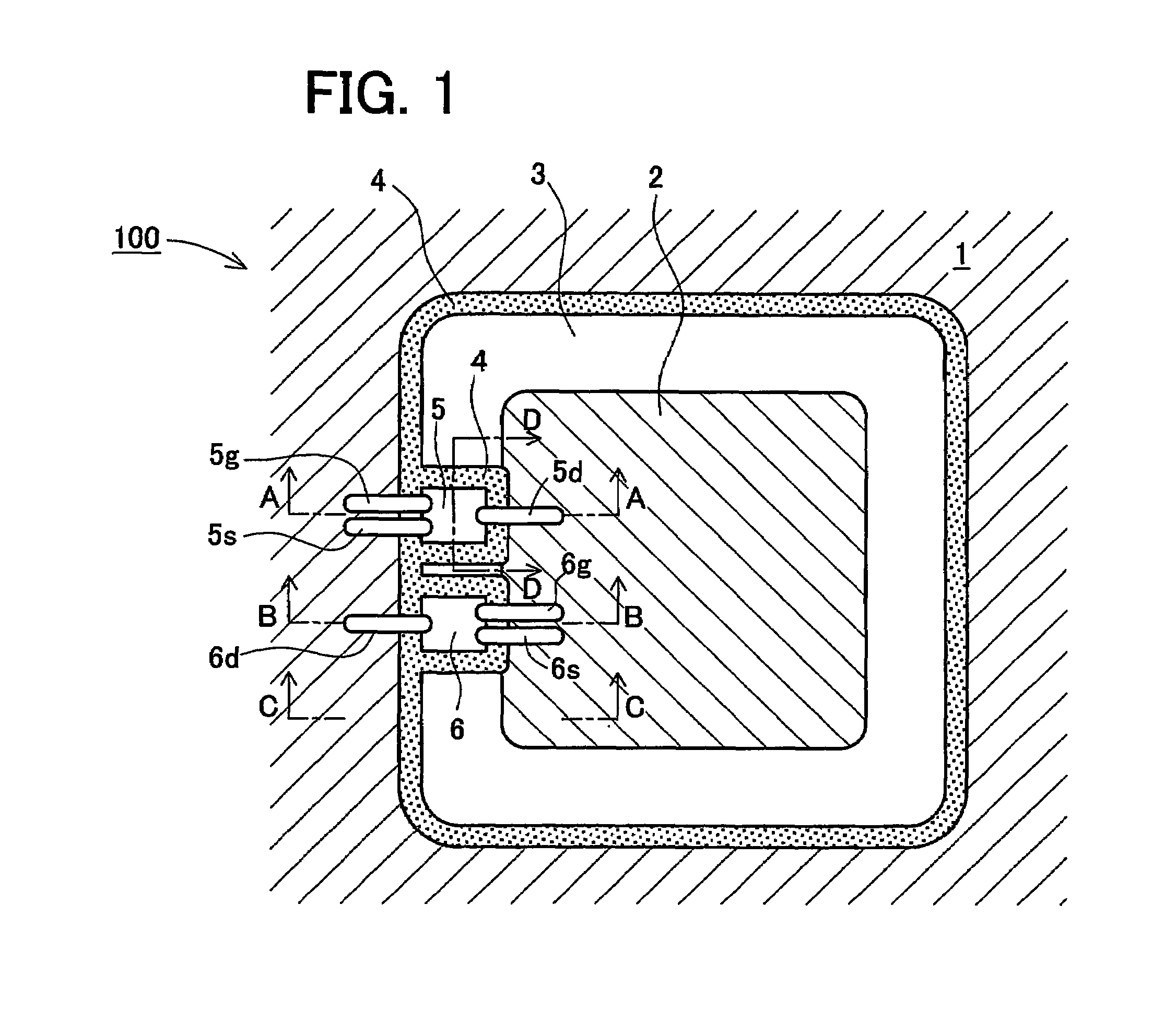
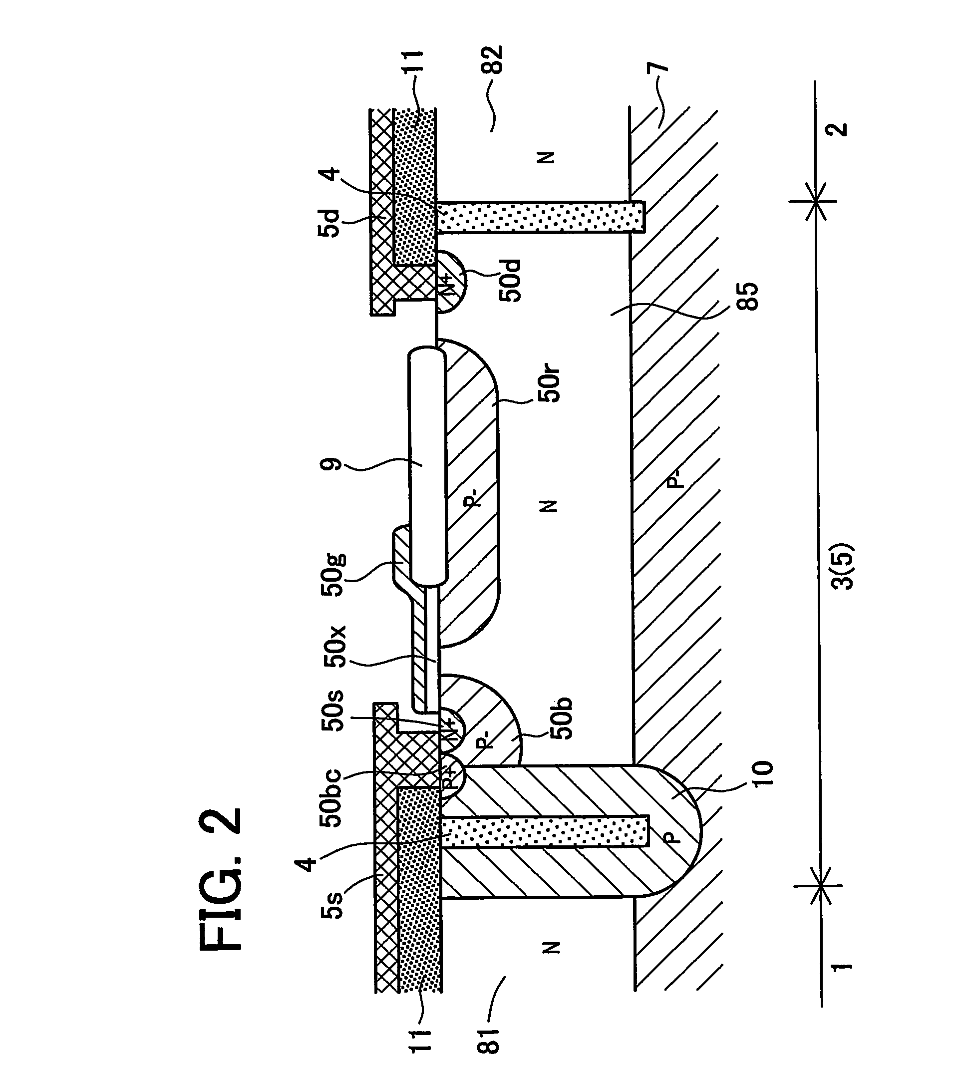
[0046]A semiconductor apparatus 100 in a first exemplary embodiment has a structure as shown in a plan view in FIG. 1. Same reference numerals as the components of the conventional semiconductor apparatus shown in FIG. 16 represent identical functions. The semiconductor apparatus 100 comprises a low potential reference circuit region 1 and a high potential reference circuit region 2, and the high potential reference circuit region 2 is surrounded by a high withstand voltage separating region 3, which is known as resurf structure. By this high withstand voltage separating region 3, the low potential reference circuit region 1 and high potential reference circuit region 2 are separated from each other. Further, a trench 4 is formed at the outer periphery of the high withstand voltage separating region 3. The trench 4 is filled up with insulating material such as silicon oxide. Accordingly, the high potential reference circuit region 2 is isolated from the low potential reference circu...

second exemplary embodiment

[0056]A semiconductor apparatus 200 in a second exemplary embodiment has a structure as shown in a plan view in FIG. 6. The semiconductor apparatus 200 comprises a low potential reference circuit region 1 and a high potential reference circuit region 2, and the high potential reference circuit region 2 is surrounded by a high withstand voltage separating region 3 same as in the semiconductor apparatus 100 in the first exemplary embodiment. Further, trenches 41, 42 are formed in part of the high withstand voltage separating region 3, and the high withstand voltage separating region 3 is partitioned into plural regions. A high withstand voltage NMOS 5 and high withstand voltage PMOS 6 are provided in the partitioned areas. What differs from the semiconductor apparatus 100 in the first exemplary embodiment is that the trenches 41, 42 do not surround completely high withstand voltage NMOS 5 and high withstand voltage PMOS 6, respectively. More specifically, trenches are not formed at th...

third exemplary embodiment

[0058]A semiconductor apparatus 300 in a third exemplary embodiment has a structure as shown in a plan view in FIG. 8. The semiconductor apparatus 300 comprises a low potential reference circuit region 1 and a high potential reference circuit region 2, and the high potential reference circuit region 2 is surrounded by a high withstand voltage separating region 3 same as in the semiconductor apparatus 100 in the first exemplary embodiment. Further, a high withstand voltage NMOS 5 is provided in part of the high withstand voltage separating region 3. An outer wall trench 43 and an inner wall trench 44 are also provided. The semiconductor apparatus 300 of this embodiment, unlike the semiconductor apparatus 100 in the first exemplary embodiment, does not have trench for partitioning the high withstand voltage separating region 3. It is hence effective to prevent lowering of withstand voltage due to crystal defects or the like likely to occur near the trench.

[0059]Only for the purpose of...


PUM


Abstract

A semiconductor apparatus (100) comprises a low potential reference circuit region (1) and a high potential reference circuit region (2), and the high potential reference circuit region (2) is surrounded by a high withstand voltage separating region (3). By a trench (4) formed in the outer periphery of the high withstand voltage separating region (3), the low potential reference circuit region (1) and high potential reference circuit region (2) are separated from each other. Further, the trench (4) is filled up with an insulating material, and insulates the low potential reference circuit region (1) and high potential reference circuit region (2). The high withstand voltage separating region (3) is partitioned by the trench (4), high withstand voltage NMOS (5) or high withstand voltage PMOS (6) is provided in the partitioned position.

Description

[0001]This is a 371 national phase application of PCT / JP2004 / 015328 filed 8 Oct. 2004, claiming priority to Japanese Application No. 2003-359229 filed 20 Oct. 2003, the contents of which are incorporated herein by reference.TECHNICAL FIELD[0002]The present invention relates to a semiconductor apparatus in which both a low potential reference circuit and a high potential reference circuit are incorporated. More particularly, it relates to a semiconductor apparatus equipped with high withstand voltage MOS which transmits signals between a low potential reference circuit and a high potential reference circuit.BACKGROUND ART[0003]There have conventionally and widely been used semiconductor apparatuses in which both a low potential reference circuit and a high potential reference circuit are incorporated for power apparatuses and the like. A semiconductor apparatus of this kind is generally structured such as shown in FIG. 16. That is, the semiconductor apparatus has a low potential refe...

Claims


Application Information

Patent Timeline
Patent Type & Authority Patents(United States)
IPC IPC(8): H01L29/72H01L21/762H01L21/76H01L21/8234H01L27/06H01L27/08H01L27/088H01L27/092H01L29/06H01L29/40H01L29/78H01L29/786
CPCH01L27/092H01L29/0649H01L29/7835H01L29/408H01L29/7801H01L29/7824H01L29/0653H01L29/0615H01L29/7816H01L21/76224H01L29/7823
Inventor TAKI, MASATOTOJIMA, HIDEKI
Owner TOYOTA JIDOSHA KK
Learn More