Gas-sensitive field-effect transistor with air gap

a field-effect transistor and air gap technology, applied in the field of gas sensors, can solve problems such as electrical short circuits, plugged diffusion channels, damage to sensitive layers,

Inactive Publication Date: 2008-12-02
MICRONAS
View PDF42 Cites 19 Cited by
  • Summary
  • Abstract
  • Description
  • Claims
  • Application Information

AI Technical Summary

Benefits of technology

[0012]Following these preparatory measures for both the substrate and the transistor, the two elements of the gas-sensitive field-effect transistor are joined by a suitable joining technology such as, for example, flip-chip methods or adhesive-bonding technology. The use of relatively thick layers makes possible applications of sensor arrangements where multiple sensors are represented on one substrate such that, for example, complex procedures, such as the detection of conflagration gas or the monitoring of ambient air quality can be achieved.

Problems solved by technology

The disadvantages of known methods of fabricating such gas sensors include the risk of damaging the sensitive layer during fabrication or of the sensor material intruding into the air gap, which factors can lead to the diffusion channel being plugged, or to electrical short circuits.

Method used


Image

  • Gas-sensitive field-effect transistor with air gap
  • Gas-sensitive field-effect transistor with air gap
  • Gas-sensitive field-effect transistor with air gap

Examples


Embodiment Construction

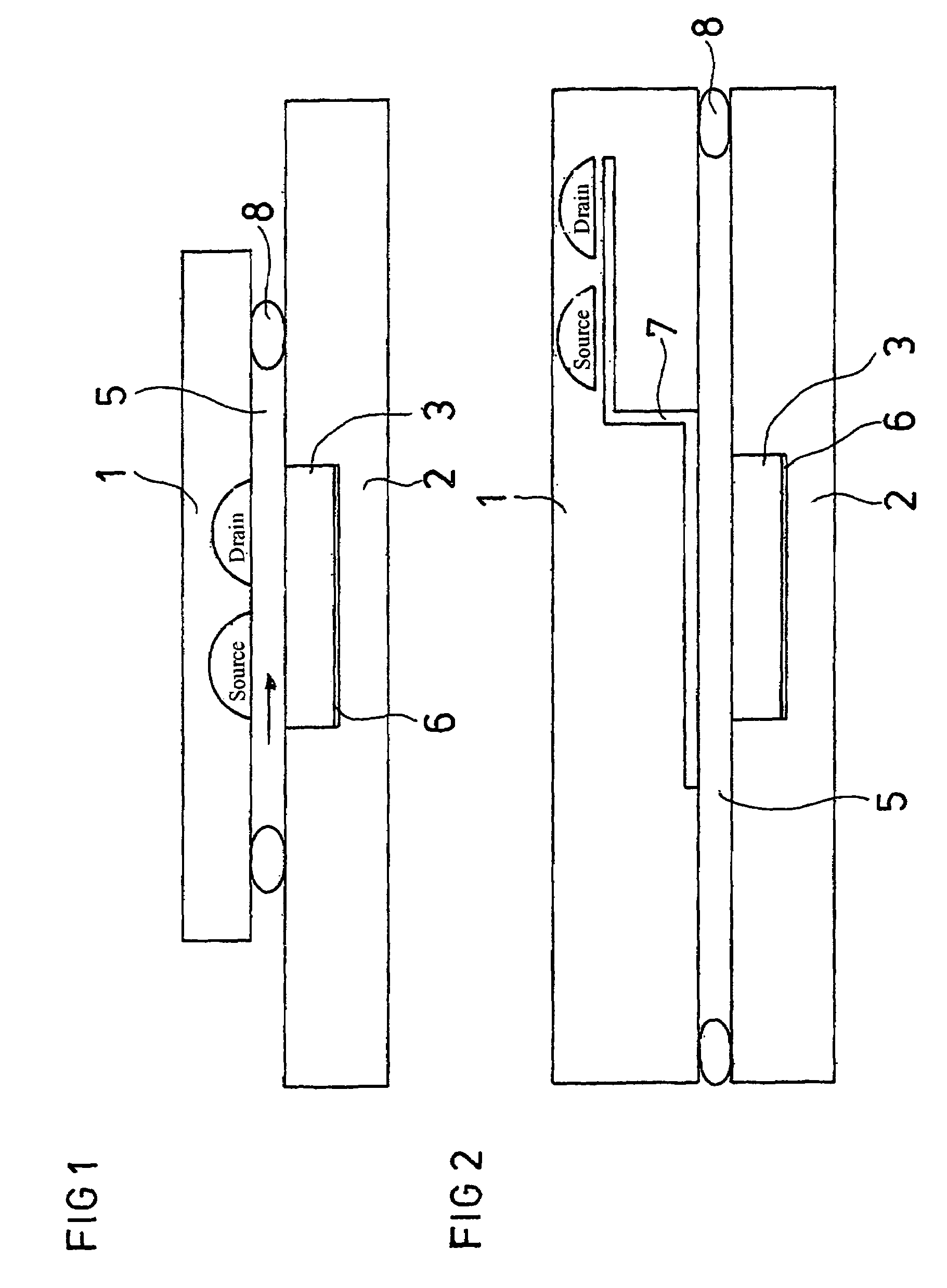
[0024]FIG. 7 illustrates a prior art SGFET 1. The diffusion of a target gas through an air gap 5, represented by polarizable oval particles, generates on a gas-sensitive layer 3 a certain potential which couples to the channel of the SGFET 1 and modifies the current between the source and the drain (IDS). The gas-sensitive layer 3 is connected to a gate electrode 6. The two tappable voltages lie between the drain and the source (UDS), and between the gate electrode 6 and the source (UGS).

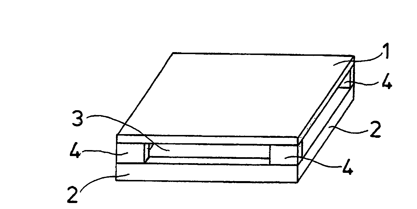
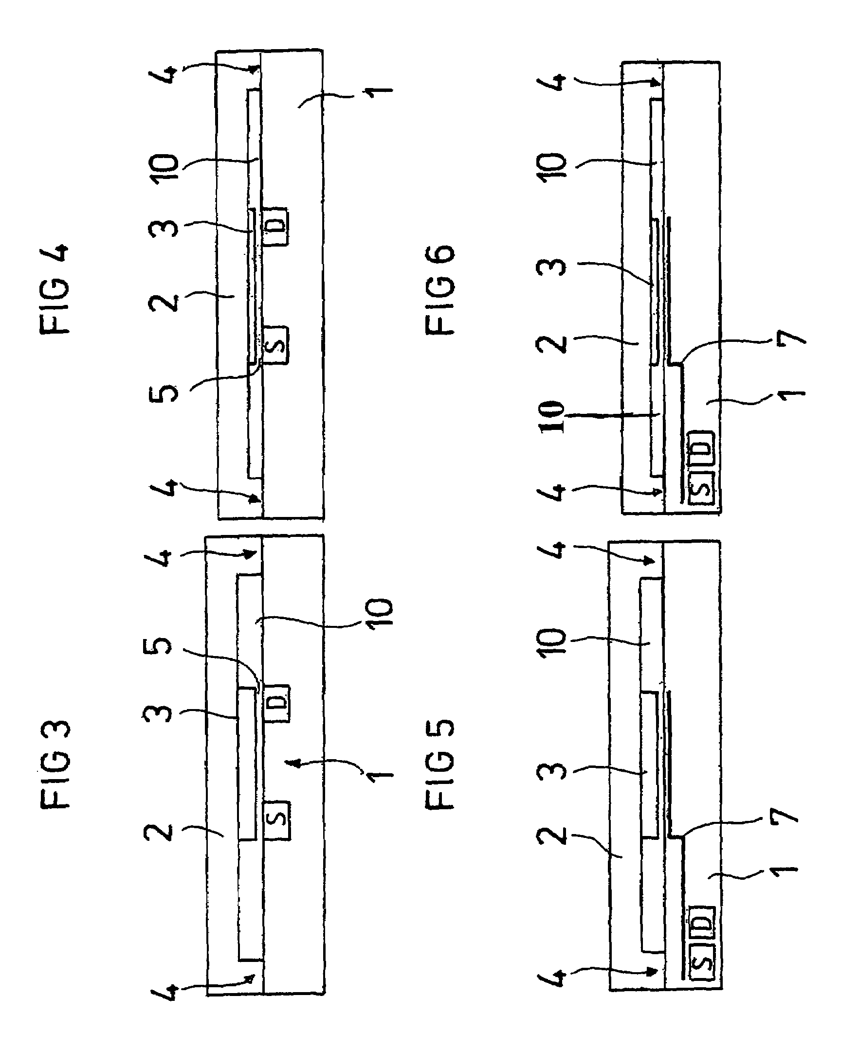
[0025]FIGS. 1-6 provide an overall view of an aspect of the gas-sensitive field-effect transistor of the present invention, with emphasis on the formation of spacers 4 on the substrate 2. If the surface precision requirements of the gas-sensitive layer 3 are relatively low, then the recess of the gas-sensitive layer 3 incorporated into the carrier substrate 2, as illustrated in FIGS. 1 and 2, can be filled in completely such that this layer 3 closes flush with the substrate surface. FIG. 1 illustrat...


PUM

PropertyMeasurementUnit
thicknessaaaaaaaaaa
heightaaaaaaaaaa
depthsaaaaaaaaaa

Abstract

A gas-sensitive field-effect transistor may be formed from a substrate with a gas-sensitive layer and a transistor processed separately and then assembled. The substrate may be patterned to form spacers by which the height of an air gap between the transistor and the sensitive layer may be adjustable to a relatively precise degree. Formation of the spacers can be achieved by patterning the substrate using material-removal techniques. The height of the spacers may be adjusted in the layer thickness of the gas-sensitive layer and for the transistor fabricated using a CMOS process. Suitable techniques for producing recesses between the spacers include, for example, polishing, cutting, sandblasting, lithographic dry etching, or wet-chemical etching. Suitable materials for the substrate may include, for example, glass, ceramic, aluminum oxide, silicon, or a dimensionally stable polymer. Following preparation of the substrate and the transistor, the two elements of the transistor are joined, for example, using flip-chip methods or adhesive-bonding technology.

Description

PRIORITY INFORMATION[0001]This patent application claims priority from German patent application 10 2005 014 763.1 filed Mar. 31, 2005, which is hereby incorporated by reference.BACKGROUND OF THE INVENTION[0002]The invention relates in general to gas sensors and in particular to a gas-sensitive field-effect transistor with an air gap.[0003]The functional principle of gas sensors based on field-effect transistors is known. When compared with other gas sensor technologies, this principle offers a number of advantages, in particular, a wide field of application as well as relatively low production and operating costs. The embodiments of the transistor known as suspended gate field effect transistor (SGFET) and capacitively controlled field effect transistor (CCFET) are especially advantageous. They are characterized by an air gap between a gate electrode and a transistor structure. The gas to be detected is diffused through the air gap and absorbed on a gas-sensitive layer. As a result...

Claims


Application Information

Patent Timeline
Patent Type & Authority Patents(United States)
IPC IPC(8): H01L27/108
CPCG01N27/002G01N27/414
Inventor FLEISCHER, MAXIMILIANLAMPE, UWEMEIXNER, HANSPOHLE, ROLANDSCHNEIDER, RALFSIMON, ELFRIEDE
Owner MICRONAS
Why Eureka
Try Eureka