Charge limited high voltage switch circuits

a high-voltage switch and circuit technology, applied in the direction of contact mechanisms, pulse techniques, instruments, etc., can solve the problems of difficult direct drive from ordinary low-voltage integrated circuits, difficult to limit the transconductance [gm] of devices, and difficult to use mosfet-based high-side switch drivers

Inactive Publication Date: 2008-11-11
MICROSEMI CORP
View PDF6 Cites 12 Cited by
  • Summary
  • Abstract
  • Description
  • Claims
  • Application Information

AI Technical Summary

Benefits of technology

[0005]The present invention envisions several ways of driving emitters in common base junction transistor stages that eliminate the need for separate high side and low side driver stages and enables drive directly from ordinary low voltage integrated circuits.

Problems solved by technology

Toward the high end of this range, however, MOSFET based high side switch drivers are problematic and expensive.
Both of these restrictions limit the transconductance [Gm] of the device.
Unfortunately, prior art driving means utilizing junction transistors have typically been arranged in a common emitter mode, often requiring separate high side or low side driver stages, and are difficult to drive directly from ordinary low voltage integrated circuits.

Method used


Image

  • Charge limited high voltage switch circuits
  • Charge limited high voltage switch circuits
  • Charge limited high voltage switch circuits

Examples


Embodiment Construction

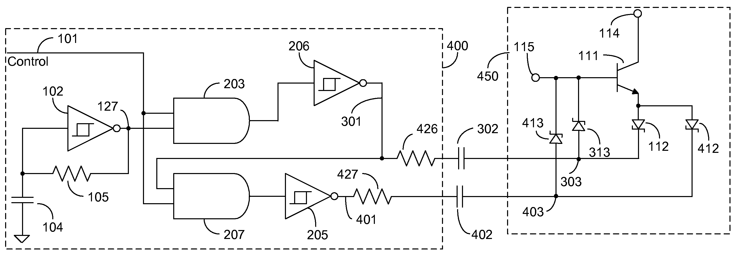
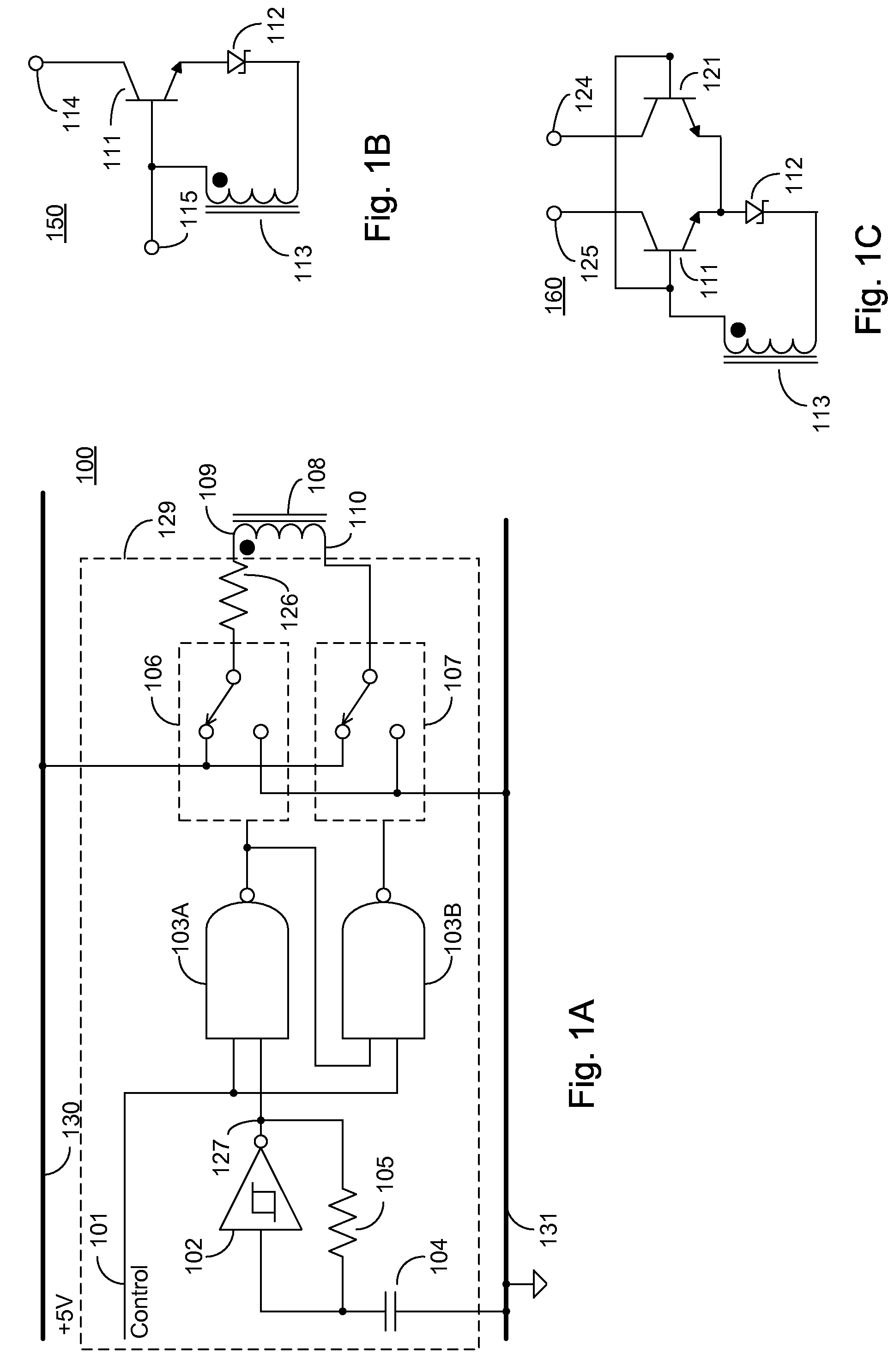
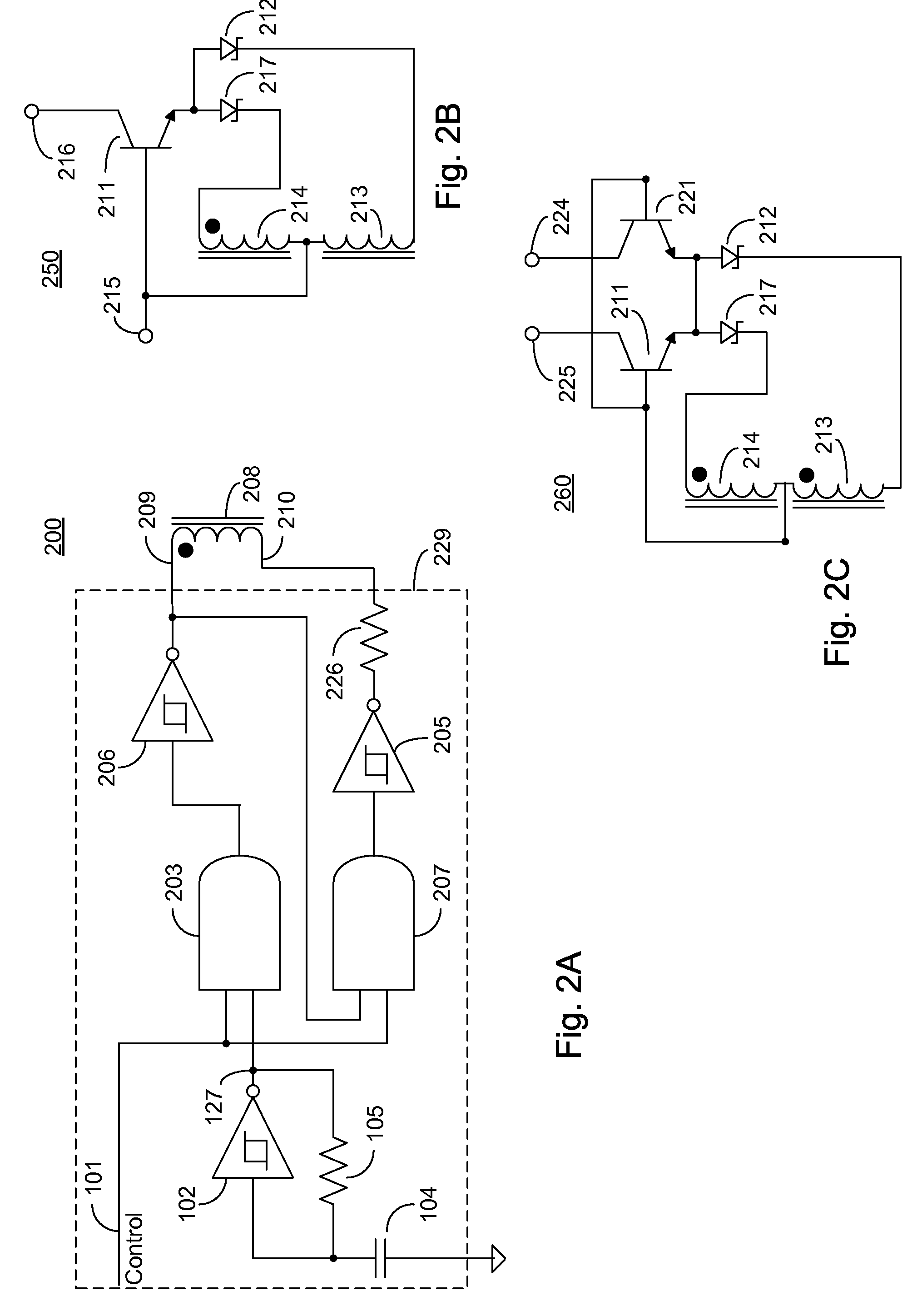
[0032]In the following description, specific details are set forth to provide a thorough understanding of the present invention. For example, specific logic functions and the circuitry for generating them may be described; however, it would be recognized by those of ordinary skill in the art that the present invention may be practiced without such specific details. In other instances, well-known circuits have been shown in block diagram form in order not to obscure the present invention in unnecessary detail. Refer now to the drawings wherein like or similar elements are designated by the same reference numeral by the several views.

[0033]The high voltage switch configurations in the following detailed description use NPN junction transistors to simplify the explanation. It is understood that a PNP junction transistor may be substituted for the NPN device by reversing the direction of the diodes and the polarity direction of the voltage source in a load circuit coupled to the high vo...


PUM


Abstract

High voltage switches are configured with a junction transistor driven with a transformer coupled AC drive signal in the common base configuration or driven by a capacitor coupled charge pump. The high voltage switches may be configured as half wave or full wave switches wherein the junction transistor is driven during one or both half cycles of the AC drive signal. Bipolar switches that can stand off high DC voltage of either polarity, or that can stand off high AC voltage, are configured from two junction transistors with their bases connected and their emitters connected. These switches may also be driven in full wave or half wave mode, by a transformer or by single or dual capacitive charge pumps. Either NPN or PNP transistors may be used. Example drive circuits, which can be constructed as low voltage integrated circuits, are given for all of the switch types.

Description

CROSS REFERENCE TO RELATED APPLICATIONS[0001]This application claims priority from U.S. Provisional Patent Application 60 / 794,500 filed Apr. 24, 2006 entitled “Charge Limited High Voltage Switch Circuits”, the entire contents of which is incorporated herein by reference.TECHNICAL FIELD[0002]The present invention relates to high voltage electronic switches, and in particular, to high voltage switches employing junction transistors.BACKGROUND INFORMATION[0003]Electronic switches represent a very great part of the advance in electronics as a whole in the last few decades, replacing metallic contacts in virtually all fast applications. All Pulse Width Modulation [PWM] power circuitry depends on fast electronic switching. At low to moderate supply voltages, typically below 50V, MOSFETs are extremely effective switches. Toward the high end of this range, however, MOSFET based high side switch drivers are problematic and expensive. At 100V and above, MOSFETs usually require 10V of drive vo...

Claims


Application Information

Patent Timeline
Patent Type & Authority Patents(United States)
IPC IPC(8): H05B41/16
CPCH03K17/61
Inventor BALL, NEWTON E
Owner MICROSEMI CORP
Why Eureka
Try Eureka