Single-mask phase change memory element

a memory element and single-mask technology, applied in the direction of digital storage, radiation control devices, semiconductor/solid-state device details, etc., can solve the problem of manufacturing such devices with very small dimensions

Active Publication Date: 2008-09-09
MACRONIX INT CO LTD
View PDF194 Cites 114 Cited by
  • Summary
  • Abstract
  • Description
  • Claims
  • Application Information

AI Technical Summary

Problems solved by technology

Problems have arisen in manufacturing such devices with very small dimensions, and with variations in process that meets tight specifications needed for large-scale memory devices.

Method used


Image

  • Single-mask phase change memory element
  • Single-mask phase change memory element
  • Single-mask phase change memory element

Examples


Embodiment Construction

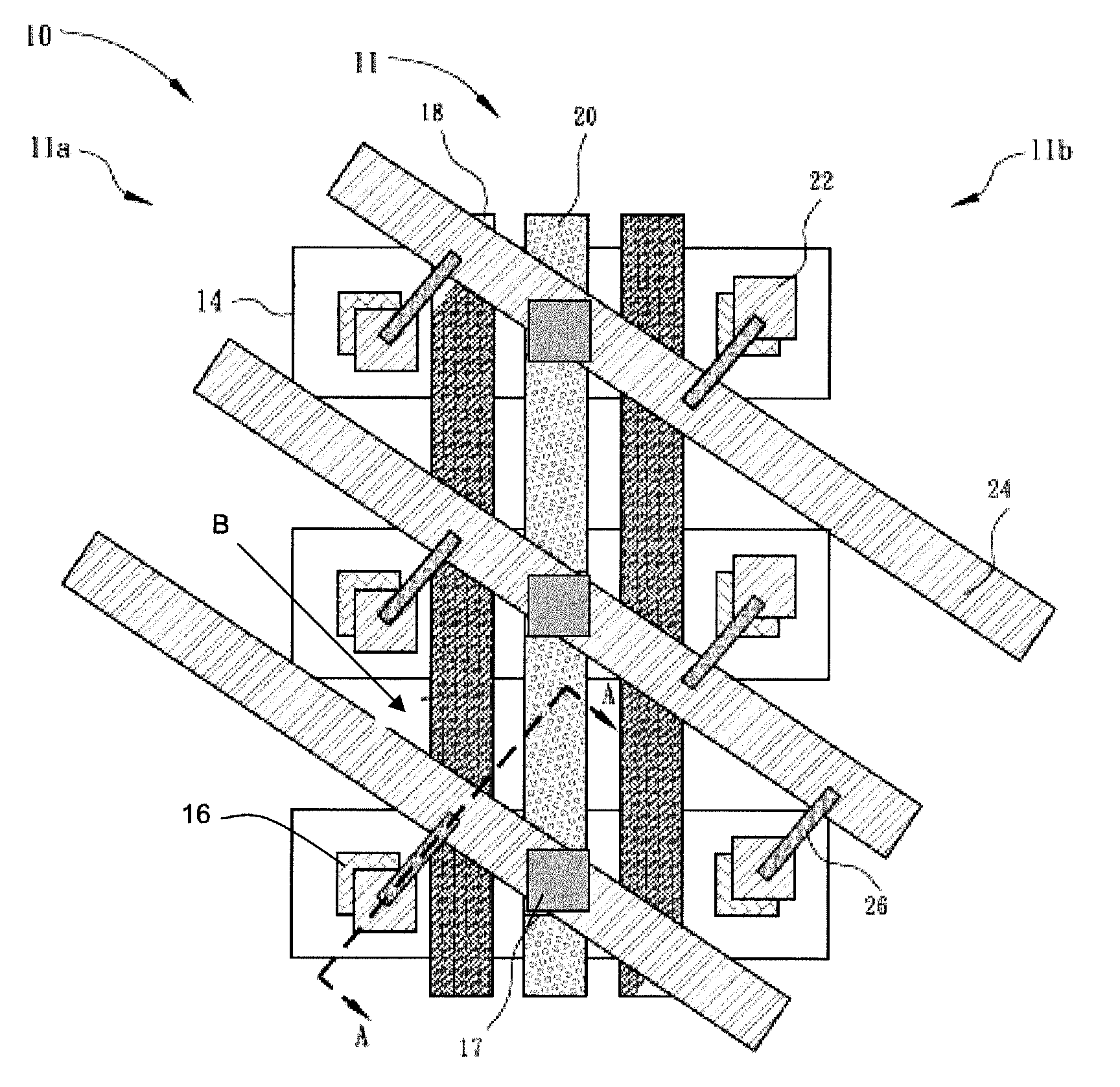
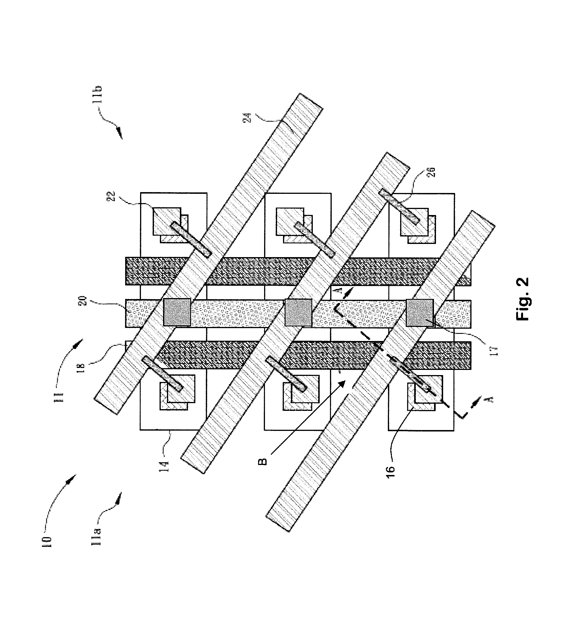
[0016]A detailed description of a memory array employing phase change memory cells, and methods for manufacturing such memory cells and arrays, is provided with reference to FIGS. 1-4. It will be understood that embodiments discussed herein and depicted in the drawings are set out for illustrative and explanatory purposes only. It is also expected that alternative embodiments and variations of embodiments will occur to those of skill in the art, in light of the explanations herein. Those and still further alternatives can fall within the scope of the present invention, which is defined solely by the claims appended hereto.

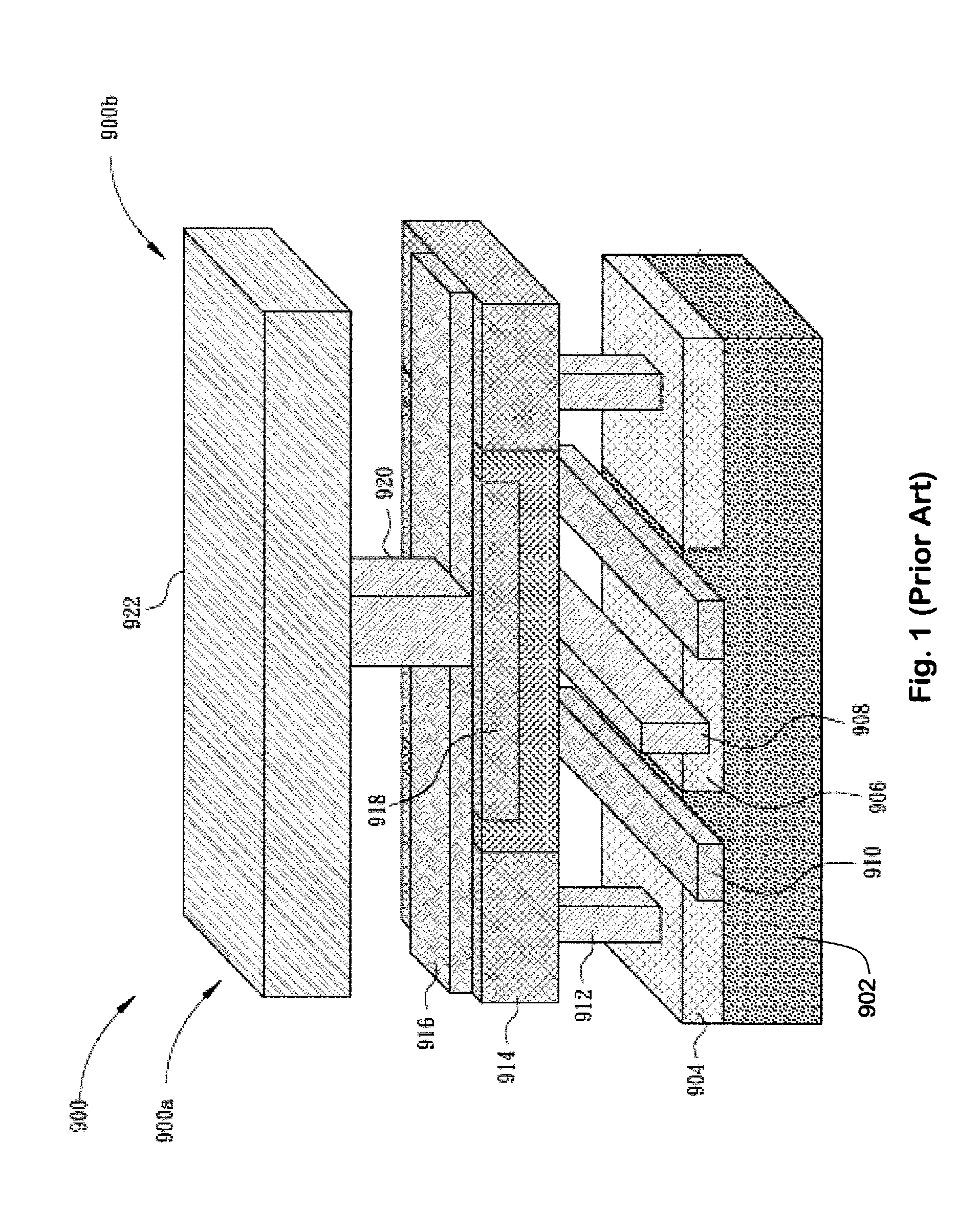
[0017]Understanding of the present application will be facilitated by consideration of known techniques for fabricating phase change memory cells. State of the art methods in this field are disclosed and taught in U.S. patent application Ser. No. 11 / 155,067 entitled “Thin Film Fuse Phase Change RAM and Manufacturing Method”, filed Jun. 17, 2005, and owned by the as...


PUM


Abstract

A memory device. An array of memory elements is formed on a semiconductor chip. A parallel array of word lines extends in a first direction, connecting each memory element to a data source, and a parallel array of bit lines extends in a second direction, connecting each memory element to a data source, the second direction forming an acute angle to the first direction. The connection between each bit line and each memory element is a phase change element composed of memory material having at least two solid phases.

Description

BACKGROUND OF THE INVENTION[0001]1. Field of the Invention[0002]The present invention relates to non-volatile memory structures, and more specifically to memory arrays employing phase change memory elements.[0003]2. Description of Related Art[0004]Phase change based memory materials are widely used in read-write optical disks and non-volatile memory arrays. These materials have at least two solid phases, including for example a generally amorphous solid phase and a generally crystalline solid phase. Laser pulses are used in read-write optical disks to switch between phases and to read the optical properties of the material after the phase change.[0005]Phase change based memory materials, such as chalcogenide based materials and similar materials, also can be caused to change phase by application of electrical current at levels suitable for implementation in integrated circuits. The generally amorphous state is characterized by higher resistivity than the generally crystalline state,...

Claims


Application Information

Patent Timeline
Patent Type & Authority Patents(United States)
IPC IPC(8): H01L27/10H01L23/48H01L29/768H01L23/52H01L27/148H01L29/73H01L29/40H01L23/58
CPCG11C11/5678H01L27/2436H01L27/2463H01L45/06H01L45/1226H01L45/144H01L45/148G11C13/0004Y10S257/907H01L2924/0002H01L2924/00H10B63/30H10B63/80H10N70/231H10N70/823H10N70/8828H10N70/884
Inventor LUNG, HSIANG-LANLIU, RICHCHEN, YI-CHOUCHEN, SHIH-HUNG
Owner MACRONIX INT CO LTD
Why Eureka
Try Eureka