Gate electrode and manufacturing method thereof, and semiconductor device and manufacturing method thereof

a manufacturing method and gate electrode technology, applied in the direction of semiconductor devices, basic electric elements, electrical apparatus, etc., can solve the problems of insufficient technique, and inability to meet the needs of mass production, and achieve excellent high frequency properties, short gate length, and fine structure

Active Publication Date: 2008-09-02
FUJITSU LTD
View PDF8 Cites 6 Cited by
  • Summary
  • Abstract
  • Description
  • Claims
  • Application Information

AI Technical Summary

Benefits of technology

[0010]In the method of manufacturing a gate electrode of the present, in the step of forming a multi-layer resist, the multi-layer resist including at least an electron beam resist layer as the lowermost layer, is formed on the surface where a gate electrode is to be formed. In the step of forming an opening, an opening is formed in layer(s) other than the lowermost layer. In the step of forming a gate electrode opening, the gate electrode opening is formed in the lowermost layer exposed from the opening. In the step of reducing a gate electrode opening, the gate electrode opening is selectively reduced. In the step of forming a gate electrode, the gate electrode is formed in the gate electrode opening. Due to this process, a high-performance, fine gate electrode can be manufactured.
[0012]Further, if a step of engraving a surface where a gate electrode is to be formed using the gate electrode opening as a mask, is included after the step of forming a gate electrode opening and before the step of reducing a gate electrode opening, a wide gate electrode opening formed in the step of forming a gate electrode opening may be used as a mask to form a recess region, and by subsequently performing the step of reducing a gate electrode opening until a desired gate electrode opening is obtained, the gate electrode can then be easily formed at a predetermined position without any offset in the recess region.
[0013]The gate electrode of the present invention is manufactured by the method of manufacturing a gate electrode of the present invention. The gate electrode has a short gate length and a fine structure, so that it can be used favorably for a field-effect transistor which has excellent high frequency properties and is useful for a transmitting and receiving device of quasi-millimeter and millimeter band waves or a high-speed signal processing (optical communication) device.
[0014]The method of manufacturing a semiconductor device of the present invention includes the method of the method of manufacturing a gate electrode of the present invention. In the method of manufacturing a semiconductor device of the present invention, a fine gate electrode can be formed, so a high-performance semiconductor device wherein a large number of field effect transistors using this gate electrode are stably assembled can be efficiently manufactured. Further, according to the method of manufacturing a gate electrode, a plurality of gate electrodes having different fineness degrees can be formed, and a plurality of offset gates in which the offset amount is optionally adjusted can also be formed, therefore, a semiconductor device having multiple functions and high-performance can be efficiently and easily manufactured.
[0015]The semiconductor device of the present invention is manufactured by the method of manufacturing a semiconductor device. The semiconductor device of the present invention includes fine gate electrodes suitable for field effect transistors or the like, and is, therefore, high-performance. Also, if a plurality of gate electrodes having different fineness degrees are provided, or a plurality of offset gates in which the offset amount is optionally adjusted are provided, the device has multiple functions together with high performance.

Problems solved by technology

However, there are the following problems in these cases.
Specifically, in (1), although in the related art it was possible to make the electron beam diameter as fine as 0.04 μm, this technique was still inadequate from the viewpoint of stable manufacture when several thousands of transistors were assembled.
In (2), because the amount of the reduction of the opening dimensions obtained stably is about 0.04 μm or less, reducing the opening dimensions drastically beyond this creates problems in the uniformity, and is not suited for mass-production.
Further, it was inherently difficult to use the same opening to form both a recess opening and gate electrode opening which have a large dimensional difference.

Method used


Image

  • Gate electrode and manufacturing method thereof, and semiconductor device and manufacturing method thereof
  • Gate electrode and manufacturing method thereof, and semiconductor device and manufacturing method thereof
  • Gate electrode and manufacturing method thereof, and semiconductor device and manufacturing method thereof

Examples


example 1

[0155]A buffer layer, InGaAs electron channel layer, AlGaAs electron supply layer and GaAs low-resistance layer were sequentially grown by MOCVD, an active region was formed by oxygen injection, and an ohmic electrode was formed using an AuGe(20 nm) / Au(200 nm) electrode.

[0156]Next, in the active region of the surface where the gate electrode is to be formed, a recess region was formed by engraving and removing low-resistance layer part in a region having a width of 0.2 μm, which region is between the both ends of the part where a fine gate (gate electrode) is to be formed.

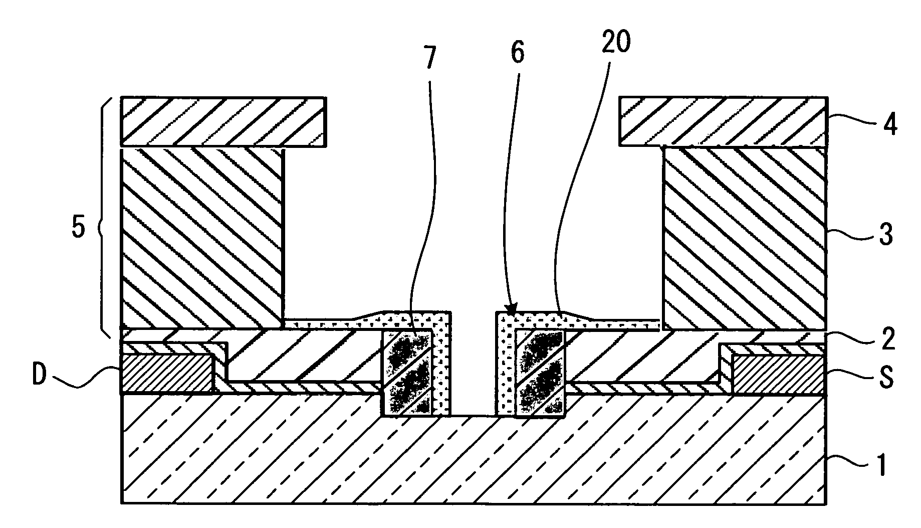
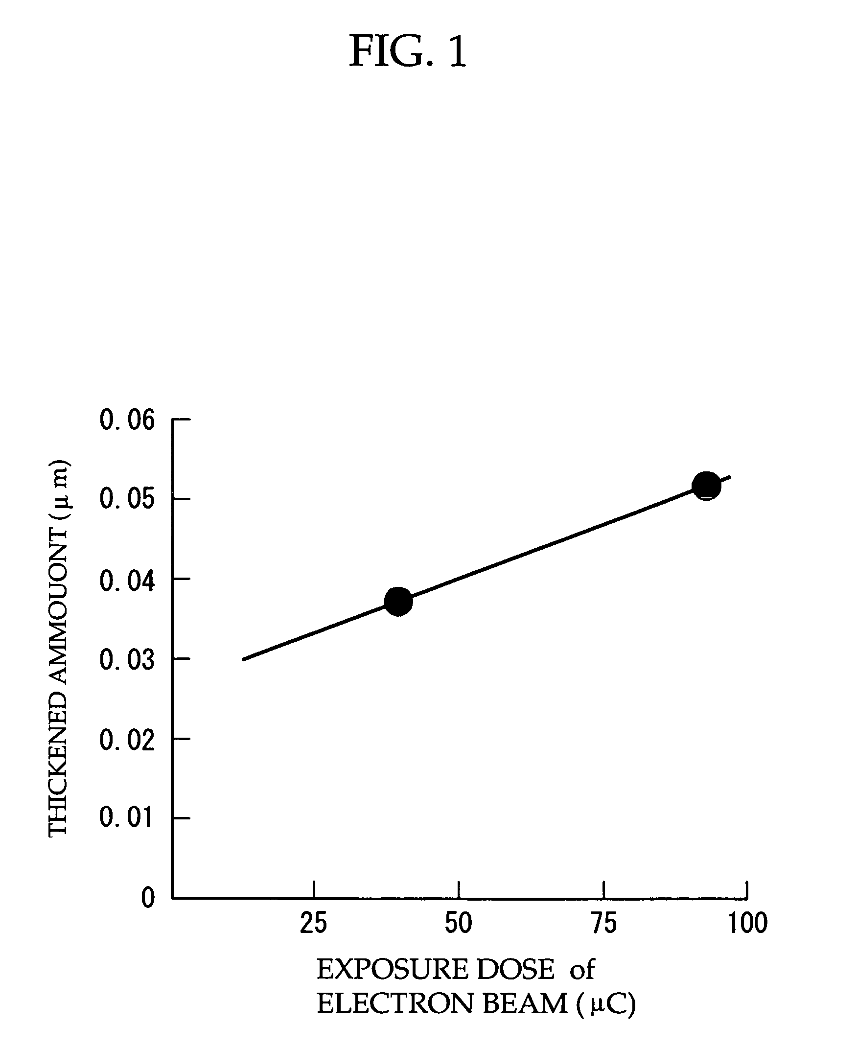
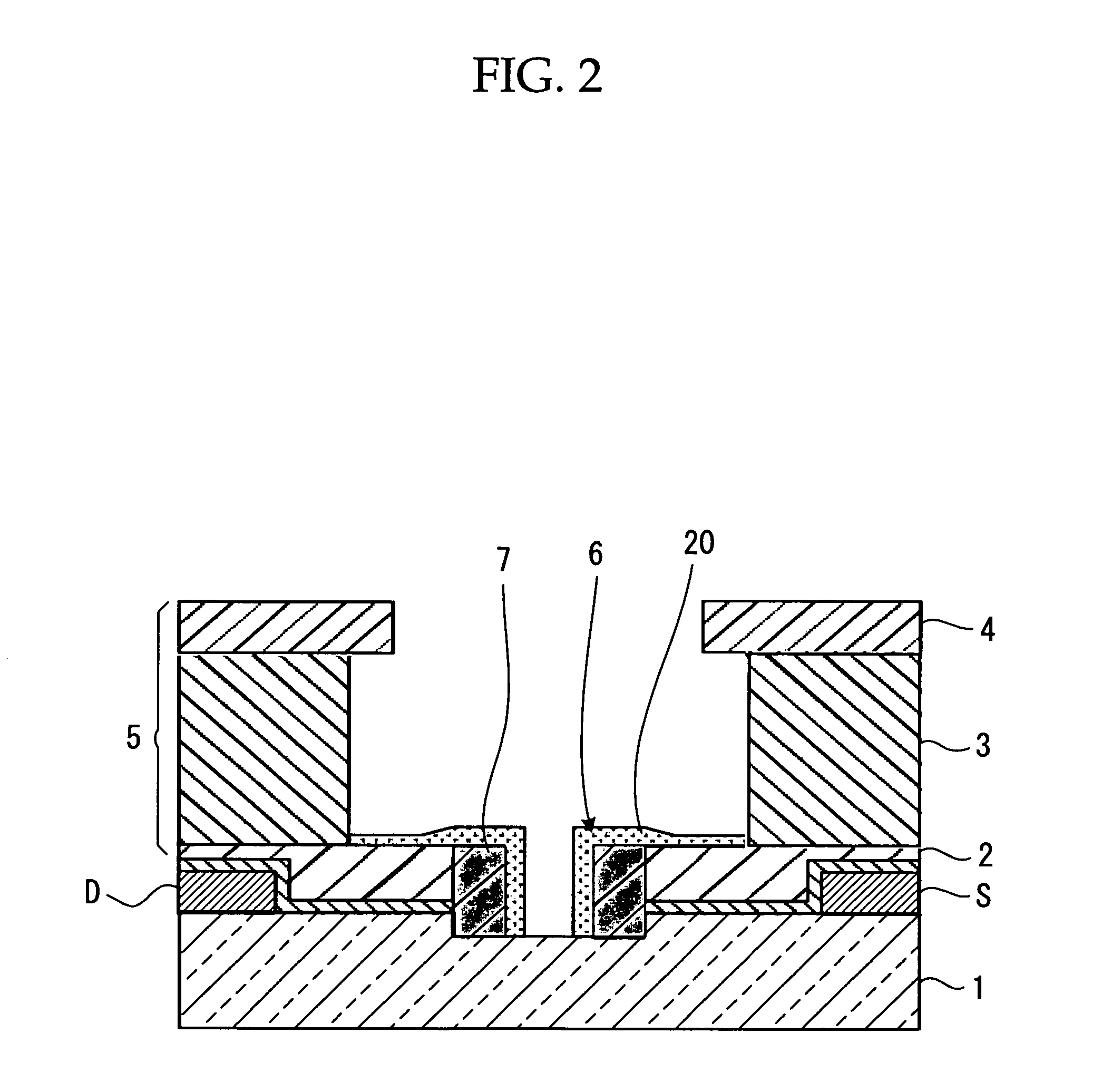
[0157]Next, as shown in FIG. 2, a PMMA resist (ZEP2000, product of Zeon Corp.) was coated by spin coating method to a thickness of 300 nm on a substrate 1 where the gate electrode is to be formed, followed by heat treatment at 180° C. for 5 minutes, to form a lowermost layer 2. PMGI (product of MicroChem Corp.) was then coated by spin coating method to a thickness of 500 nm thereupon, followed by heat treatment at ...

example 2

[0165]This example is identical to Example 1, except that the step of engraving the surface where a gate electrode is to be formed in Example 1 is performed after the step of forming a gate electrode opening, and before the step of exposing to an electron beam and step of reducing a gate electrode opening.

[0166]Specifically, as shown in FIG. 4A, a source electrode S and drain electrode D were formed at a fixed interval on the surface of a semiconductor substrate, and the SiN film was deposited on the surface of semiconductor substrate. The multi-layer resist 5 comprising the lowermost layer 2, intermediate layer 3 and uppermost layer 4 was then formed on the SiN film by the step of forming a multi-layer resist. Next, an opening was formed in the uppermost layer 4 and the intermediate layer 3 in the multi-layer resist 5 by the step of forming an opening. A gate electrode opening 10 having opening dimensions of 0.2 μm was then formed by the step of forming a gate electrode opening.

[01...

example 3

[0171]In the step of exposing to an electron beam in Example 2, in order to selectively reduce the opening dimensions on the drain electrode D side in the gate electrode opening, only the drain electrode D side was exposed to a dose (60 μC) below the developing Eth (FIGS. 5A to 5C).

[0172]As a result, as shown in FIG. 5D, a field effect transistor having an offset gate in which the recess length on the drain electrode D side was 0.04 μm longer than the recess length on the source electrode S side with respect to the gate electrode 30, was obtained.

[0173]The present invention provides a method of manufacturing a gate electrode in which a fine gate electrode can effectively be manufactured by thickening a resist opening for gate electrodes formed by ordinary electron beam lithography so as to reduce opening dimensions. The present invention also provide a gate electrode which is manufactured by the method of manufacturing a gate electrode and is used favorably for a field-effect transi...


PUM


Abstract

The present invention provides a method of manufacturing a gate electrode in which a fine gate electrode can effectively be manufactured by thickening a resist opening for gate electrodes formed by ordinary electron beam lithography so as to reduce opening dimensions. The method of manufacturing a gate electrode of the present invention includes a step of forming a laminated resist including at least an electron beam resist layer as a lowermost layer on a surface where a gate electrode is to be formed; a step of forming an opening in layer(s) other than the lowermost layer; a step of forming a gate electrode opening on the lowermost layer exposed from the opening; a step of reducing the gate electrode opening selectively; and a step of forming a gate electrode in the gate electrode opening.

Description

CROSS-REFERENCE TO RELATED APPLICATIONS[0001]This is a continuation of Application PCT / JP2003 / 009865, filed on Aug. 4, 2003.BACKGROUND OF THE INVENTION[0002]1. Field of the Invention[0003]The present invention relates to a method of manufacturing a gate electrode in which a fine gate electrode can effectively be manufactured by thickening a resist opening for gate electrodes formed by ordinary electron beam lithography so as to reduce opening dimensions, to a gate electrode which is manufactured by the method of manufacturing a gate electrode and is used favorably for a field-effect transistor which has excellent high frequency properties and is useful for a transmitting and receiving device of quasi-millimeter and millimeter band waves or a high-speed signal processing (optical communication) device, and to a semiconductor device using the gate electrode and method of manufacturing thereof.[0004]2. Description of the Related Art[0005]Field-effect transistors having superior high fr...

Claims


Application Information

Patent Timeline
Patent Type & Authority Patents(United States)
IPC IPC(8): H01L21/28H01L21/027H01L29/423
CPCH01L21/0277H01L29/42316H01L21/28Y10S438/95
Inventor MAKIYAMA, KOZONOZAKI, KOJI
Owner FUJITSU LTD
Why Eureka
Try Eureka