Clock generator for semiconductor memory apparatus

a clock generator and memory technology, applied in the direction of generating/distributing signals, instruments, pulse techniques, etc., can solve the problems of reducing the reliability of the clock, difficult to correct the clock phase, and frequent clock generating errors, so as to achieve stable and reliable clocks

Active Publication Date: 2008-08-19
SK HYNIX INC
View PDF13 Cites 11 Cited by
  • Summary
  • Abstract
  • Description
  • Claims
  • Application Information

AI Technical Summary

Problems solved by technology

In the clock generator for a semiconductor memory apparatus according to the related art, a clock period becomes shorter as the speed of the operation of the semiconductor memory apparatus becomes higher, which causes a problem in that it is difficult to correct the phase of the clock, and thus a clock generating error frequently occurs.
In addition, the related art has a problem in that the reliability of the clock is lowered due to the frequent clock errors and a system using the clock generator may operate incorrectly.

Method used


Image

  • Clock generator for semiconductor memory apparatus
  • Clock generator for semiconductor memory apparatus
  • Clock generator for semiconductor memory apparatus

Examples


Embodiment Construction

[0027]Hereinafter, a clock generator for a semiconductor memory apparatus according to a preferred embodiment of the present invention will be described with reference to the accompanying drawings.

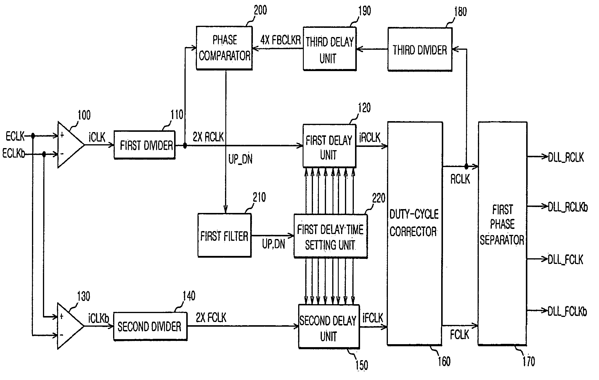
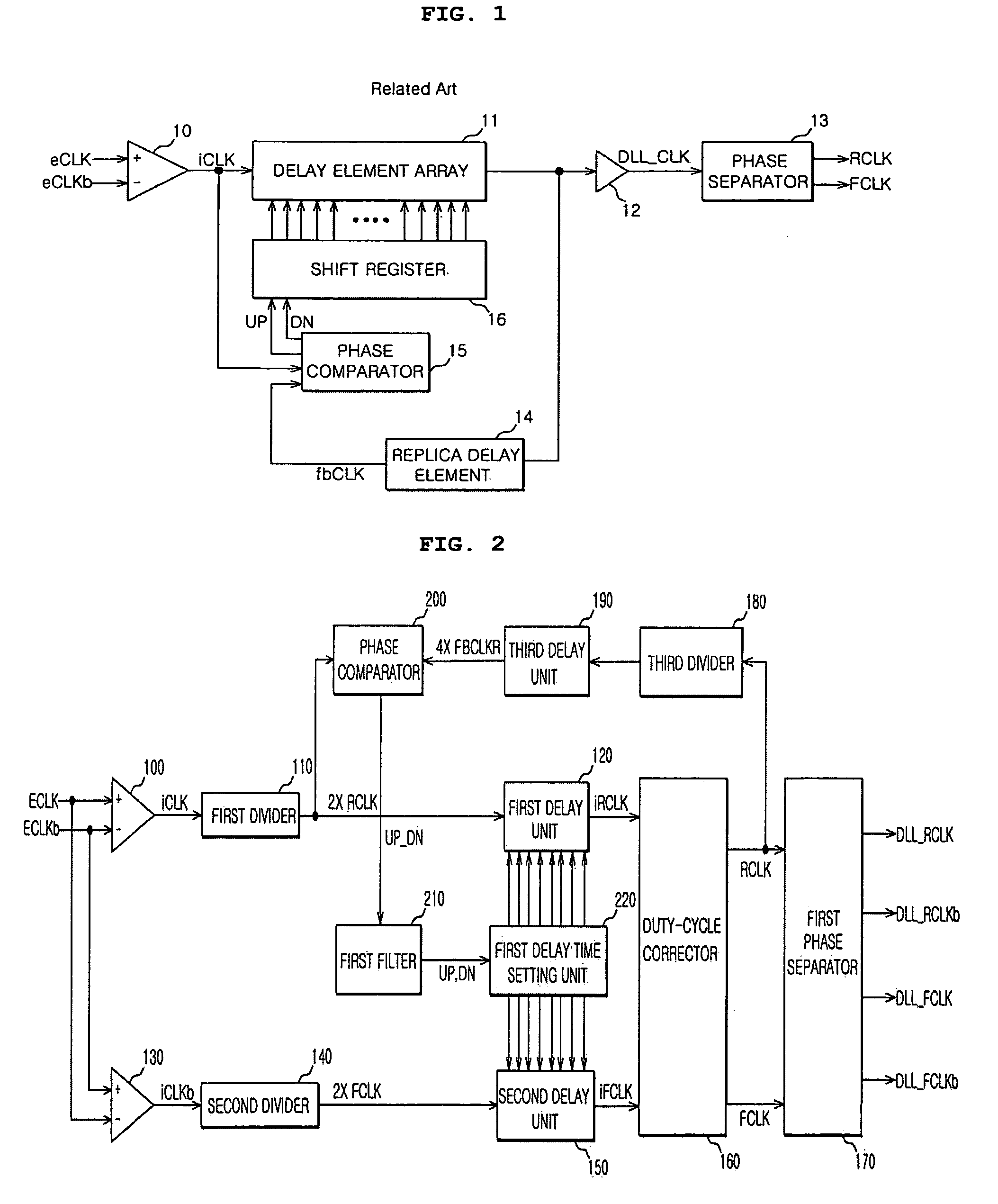
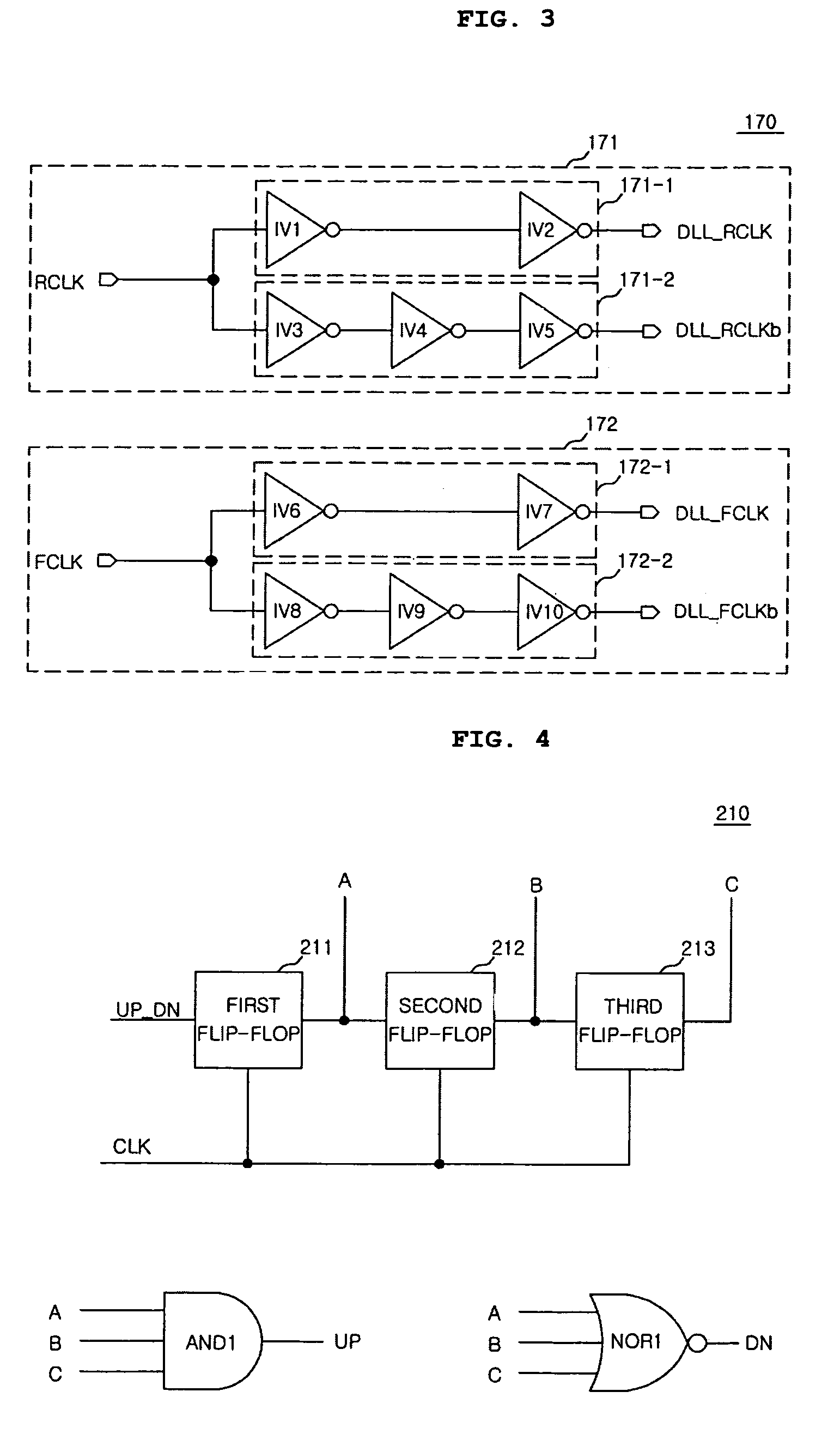
[0028]FIG. 2 is a block diagram showing the configuration of a clock generator for a semiconductor memory apparatus according to an embodiment of the present invention. FIG. 3 is a circuit diagram showing the configuration of a first phase separator shown in FIG. 2. FIG. 4 is a circuit diagram showing a first LPF shown in FIG. 2. FIG. 5 is a block diagram showing the configuration of a duty-cycle corrector shown in FIG. 2. FIG. 6 is a circuit diagram showing the configuration of a duty detector shown in FIG. 5. FIG. 7 is a timing chart for illustrating the operation of the clock generator for a semiconductor memory apparatus according to an embodiment of the present invention. FIG. 8 is a timing chart for illustrating the operation of the duty-cycle corrector shown in FIG. 2.

[0029]As shown...


PUM


Abstract

The clock generator for semiconductor memory apparatus which includes: a first divider; a first delay unit; a second divider; a second delay unit; a duty-cycle corrector; a third divider; a third delay unit; a phase comparator; and a delay time setting unit. The clock generator for semiconductor memory apparatus exactly performs phase correction and duty cycle correction using frequency-divided clocks. Therefore, it is possible to generate reliable clocks and to improve the operational performance of a system using the clock generator.

Description

BACKGROUND OF THE INVENTION[0001]1. Technical Field[0002]The present invention relates to a semiconductor memory apparatus. In particular, the present invention relates to a clock generator for a semiconductor memory apparatus.[0003]2. Related Art[0004]In general, a DLL (Delay Locked Loop) is a clock generator compensating for a skew between an external clock and data or between an external clock and an internal clock.[0005]A clock generator according to the related art includes a clock receiver 10, a delay element array 11, a buffer 12, a phase separator 13, a replica delay element 14, a phase comparator 15, and a shift register 16, as shown in FIG. 1.[0006]The clock receiver 10 receives external clock eCLK and inverted external clock eCLKb having phase opposite to the external clock and outputs an internal clock iCLK.[0007]The delay element array 11 is composed of a plurality of delay elements. The delay element array 11 delays the internal clock iCLK by a delay time of a delay el...

Claims


Application Information

Patent Timeline
Patent Type & Authority Patents(United States)
IPC IPC(8): G06F1/04
CPCG11C7/22H03L7/0814G11C7/222H03K2005/00241H03L7/0816G11C11/4076G11C8/18
Inventor LEE, HYUN-WOO
Owner SK HYNIX INC
Why Eureka
Try Eureka