Apparatus and method for characterizing pulsed optical signals

a pulsed optical and signal technology, applied in the field of communication signals, can solve the problems of affecting the quality of optical signals, and reducing the accuracy of optical signals, so as to achieve the effect of reducing the difficulty of optical signal processing

Inactive Publication Date: 2008-07-29
LUMENTUM OPERATIONS LLC
View PDF6 Cites 10 Cited by
  • Summary
  • Abstract
  • Description
  • Claims
  • Application Information

AI Technical Summary

Benefits of technology

[0009]An object of the present invention is to provide a simpler optical set-up based on two-beam interference effect to test the eye opening of a high speed digital communication system, especially over 10 GBit / second, without having to rely on speed-limited and costly electronic solution. The current invention is in favor of high speed, which means shorter time delay in one of the two arm of the interferometer required for interference amplitude profile measurement.

Problems solved by technology

In newer digital optical communication systems operating at higher speeds of bit rates at 10 Gbits / sec or more, monitoring the signal quality deterioration becomes more problematic with increasing bit rates.
Conventional methods involving the electronic measurement and subsequent processing of the optical signal eye diagram will be limited by the inherent difficulties in performing electronic processing at very high bit rates, rendering such methods to be prohibitively expensive for bit rates in excess of about 10 Gbits / sec.
The ability to use optical sampling before conversion to electronic signal facilitates the use of less sophisticated electronic processing: Reliance upon the organic non-linear crystal, however, has inherent disadvantages such as the difficulty of integrating this optical component in a sensor system.
A further major disadvantage of this method is that sampling pulses are required to be generated at excessively high power, i.e. in excess of 200 watts.
Again the use of semiconductor devices in this disclosure may present practical limitations with optical signals at very high bit rates.

Method used


Image

  • Apparatus and method for characterizing pulsed optical signals
  • Apparatus and method for characterizing pulsed optical signals
  • Apparatus and method for characterizing pulsed optical signals

Examples


Embodiment Construction

[0061]Reference herein to any embodiment means that a particular feature, structure, or characteristic described in connection with the embodiment can be included in at least one embodiment of the invention. The appearances of the phrase “in one embodiment” in various places in the specification are not necessarily all referring to the same embodiment, nor are separate or alternative embodiments mutually exclusive of other embodiments.

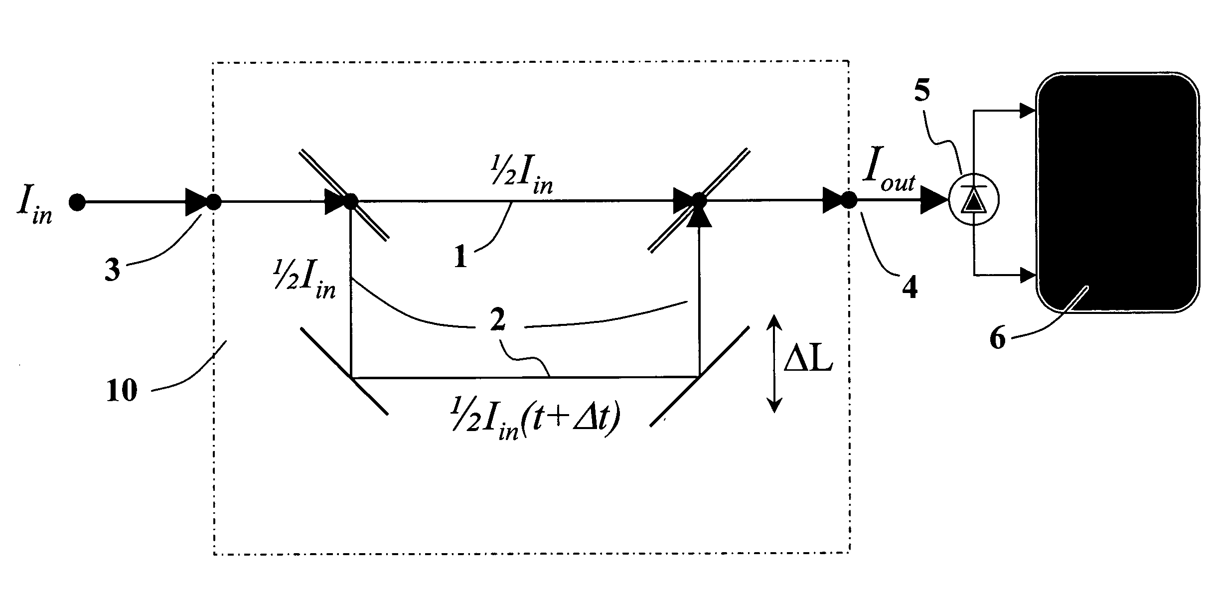
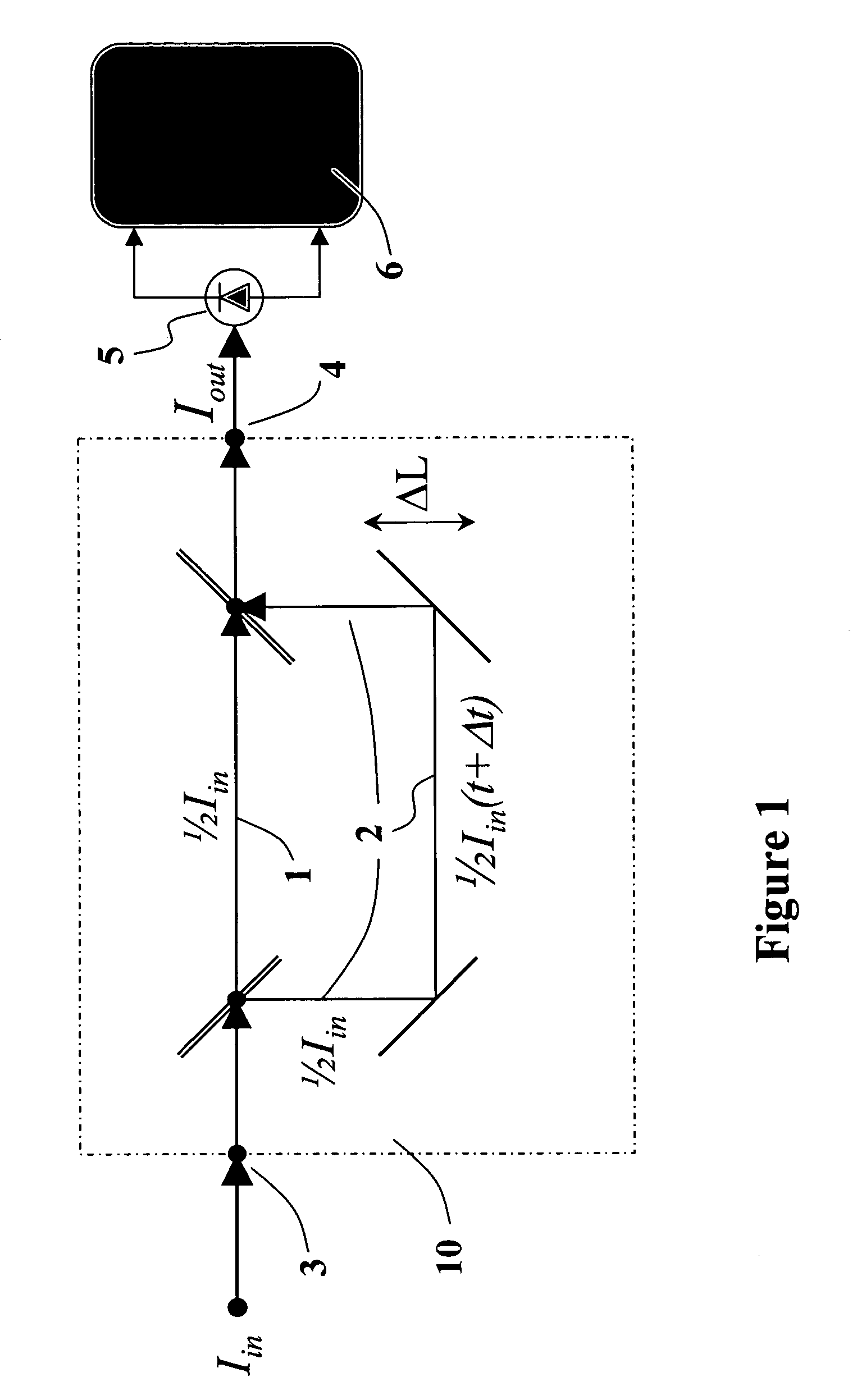
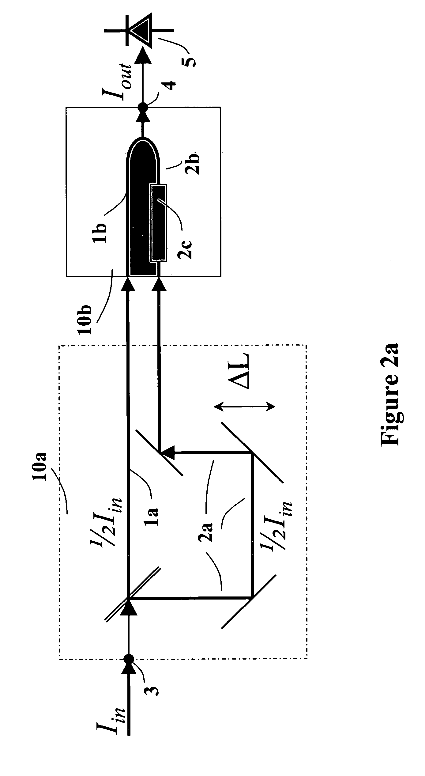
[0062]The present invention addresses the limitations of prior art systems by making use of the fact that the coherence length of a light beam forming original optical signal bits is much larger than the coherence length of the added optical noise. This makes it possible to separate the bit signal level from noise by using coherent interference effect.

[0063]FIG. 1 illustrates the process of obtaining an interference signal from combining two analogous signals derived from a detected signal in a communication system in general, and a pulsed optical sign...


PUM


Abstract

The coherent interference effect between two beam is used with one light beam delayed by a controllably variable time delay with respect to another analogous beam to obtain a convolutional profile of the oscillatory component of the interference amplitude as a function of the time delay, having a peak value representing the performance clearance between a zero-bit and a one-bit. The convolutional profile is represented by a diamond diagram (DD) of the interference amplitude, within the coherence length. The peak value and the size of DD openings are used for characterizing pulsed optical signals by determining at least one of a predefined set of signal parameters, including signal degradation, optical chromatic dispersion, signal coherence length, type of signal modulation, and signal-to-noise ratio. The two-beam interference effect is optionally provided by a free-space Mach Zehnder interferometer, an integrated Mach Zehnder interferometer, a Michelson interferometer, or combinations thereof.

Description

CROSS-REFERENCE TO RELATED APPLICATIONS[0001]The present invention claims priority from U.S. Provisional Patent Application No. 60 / 691,443 filed Jun. 17, 2005, and entitled “Optical Detection on Communication Eye Diagram Using Coherent Interference Effect”, which is incorporated herein by reference.FIELD OF THE INVENTION[0002]This invention generally relates to systems and methods for characterizing communication signals in general, and of high-speed pulsed optical signals in particular.BACKGROUND TO THE INVENTION[0003]In newer digital optical communication systems operating at higher speeds of bit rates at 10 Gbits / sec or more, monitoring the signal quality deterioration becomes more problematic with increasing bit rates. Conventional methods involving the electronic measurement and subsequent processing of the optical signal eye diagram will be limited by the inherent difficulties in performing electronic processing at very high bit rates, rendering such methods to be prohibitivel...

Claims


Application Information

Patent Timeline
Patent Type & Authority Patents(United States)
IPC IPC(8): G01B9/02H04B10/07H04B10/075H04B10/2507H04B10/556
CPCH04B10/07953
Inventor SHEN, JINXI
Owner LUMENTUM OPERATIONS LLC
Why Eureka
Try Eureka