
Method of fabricating near field optical probe

a near field, optical probe technology, applied in the field of near field optical probes, can solve the problems of etching silicon inside the tip or boring the hole of the tip, the substrate supporting the cantilever and the sample may collide, and the process is difficul

Inactive Publication Date: 2008-07-01
ELECTRONICS & TELECOMM RES INST
View PDF5 Cites 11 Cited by
  • Summary
  • Abstract
  • Description
  • Claims
  • Application Information

AI Technical Summary

Benefits of technology

[0017]The present invention is also directed to a near-field optical probe having an optical tip facing an upper face of the substrate to prevent collision with the sample.

Problems solved by technology

However, the near-field probes having the arrangement described above has a chance that the substrate supporting the cantilever and the sample may be collided when the cantilever is moved and the probe is close to the sample.
In this case, a process of arranging and aligning the tip and the cantilever is further required, which accompanies the difficulty in the process.
However, there is a difficulty in etching the silicon inside the tip or boring the hole of the tip.
In other words, though it is necessary to maintain a constant thickness of the substrate during the silicon process, there is a difficulty in proceeding the process since the backside of the tip should be patterned after the most portion of the backside of the substrate is removed to form the cantilever.
However, in this case, the high-cost apparatus is required.
However, with the probe comprising the optical fiber, the arrangement of the probe is mechanically weak, and it is difficult to fabricate the multiple probes.

Method used


Image

  • Method of fabricating near field optical probe
  • Method of fabricating near field optical probe
  • Method of fabricating near field optical probe

Examples


Embodiment Construction

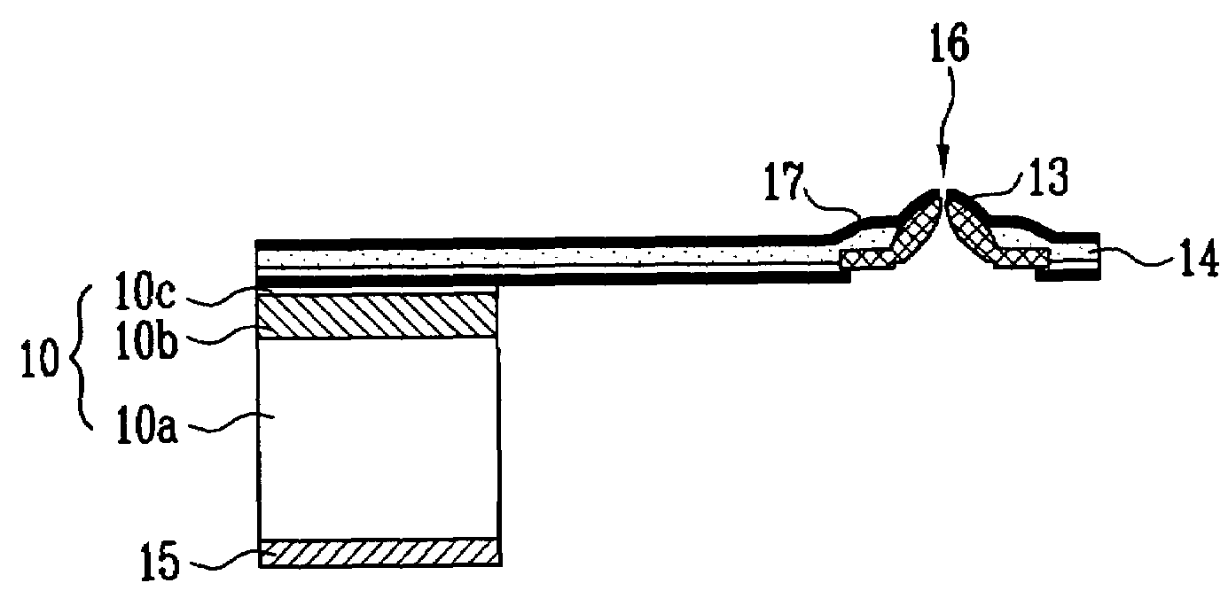
[0029]Exemplary embodiments of the present invention will now be described more fully with reference to the accompanying drawings. This invention may, however, be embodied in different forms and should not be construed as limited to the embodiments set forth herein. Rather, these embodiments are provided so that this disclosure will be thorough and complete, and will fully convey the scope of the invention to those skilled in the art.

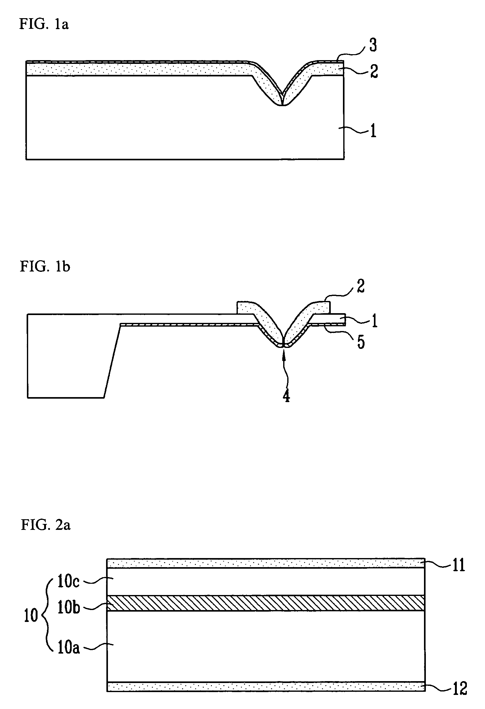
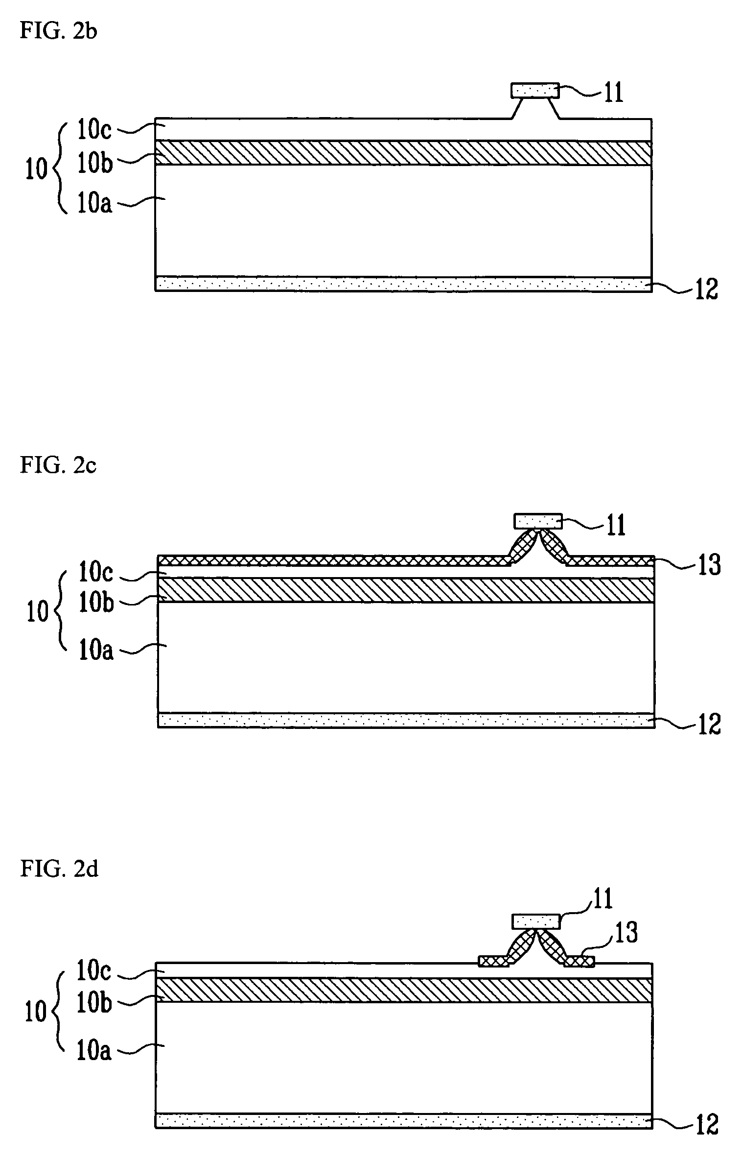
[0030]FIGS. 2A and 2N are diagrams for explaining a method of fabricating the conventional near-field optical probe according to an exemplary embodiment the present invention.

[0031]Referring to FIG. 2A, silicon nitride layers 11 and 12 are deposited in about 300 nm on both sides of the substrate 10 having silicon on insulator (SOI) by using a low pressure chemical vapor deposition (LPCVD) method.

[0032]The SOI substrate 10 comprises a lower silicon layer 10a, a silicon oxide layer 10b and an upper silicon layer 10c, subsequently deposited.

[0033]Referring...


PUM

PropertyMeasurementUnit
widthaaaaaaaaaa
widthaaaaaaaaaa
temperatureaaaaaaaaaa

Abstract

Provided is a method of fabricating a near-field optical probe adapted to a near-field scanning optical microscopy and a near-field information storage device, in which a cantilever and an optical tip are provided in one body and the optical tip is arranged to face the upper portion of the substrate. High-concentrated boron ions are implanted into an uppermost silicon layer of a silicon on insulator (SOI) substrate, and a silicon layer into which boron ions are implanted while the silicon inside the tip is etched to form the hole to act as an etch stop layer, thereby easily removing the silicon inside the tip even with the cantilever exposed, and simplifying the process due to the simultaneous fabrication of the cantilever and the tip.

Description

CROSS-REFERENCE TO RELATED APPLICATION[0001]This application claims priority to and the benefit of Korean Patent Application No. 2004-26951, filed on Apr. 20, 2004, the disclosure of which is incorporated herein by reference in its entirety.BACKGROUND[0002]1. Field of the Invention[0003]The present invention relates to a method of fabricating a near field optical probe employed to a near field scanning optical microscopy and near field information storage device and, more specifically, to a method of fabricating a near-field optical probe in which a cantilever and an optical tip are provided in one body and the optical tip is arranged to face the upper portion of the substrate.[0004]2. Discussion of Related Art[0005]After an atomic force microscopy was invented, a research has been widely conducted on applications of a scanning probe microscopy (SPM) capable of measuring optical, electrical, and magnetic characteristics of a sample in a nanometer resolution. The atomic force microsc...

Claims


Application Information

Patent Timeline
Patent Type & Authority Patents(United States)
IPC IPC(8): H01L21/00G01Q60/22B44C1/22G01Q70/18G11B7/135G11B7/1387G11B9/14
CPCB82Y20/00G11B7/1387G01Q60/22B82Y35/00F16L41/021F16L19/02
Inventor KIM, EUN KYOUNGLEE, SUNG QSONG, KI BONGPARK, KANG HO
Owner ELECTRONICS & TELECOMM RES INST
Learn More