
Apparatus and methods for the detection of an arc in a plasma processing system

a plasma processing system and apparatus technology, applied in the direction of vibration measurement in solids, manufacturing tools, instruments, etc., can solve the problems of increasing the risk of dielectric breakdown and arcing between the components, arcing that neither consumes enough energy nor exists for a sufficient length of time to generate a distinguishable signal,

Active Publication Date: 2008-02-26
LAM RES CORP
View PDF7 Cites 46 Cited by
  • Summary
  • Abstract
  • Description
  • Claims
  • Application Information

AI Technical Summary

Problems solved by technology

The high density of components in these advanced integrated circuits increases the risk of dielectric breakdown and arcing between the components, or between the components and the plasma during plasma processing.
This may result in damage to the substrate as well as the plasma chamber.
However, an arc can occur that neither consumes enough energy nor exists for a sufficient length of time to generate a distinguishable signal from the background plasma process noise (e.g., signal-to-noise ratio).
Such arcing can still cause failure of the circuit being manufactured and collateral damage to other circuits and portions of the substrate.
Likewise, the small perturbation of the plasma light intensity due to the arc is less than the normal intensity fluctuations in the plasma; hence, spectroscopic detection of the arc also has poor signal-to-noise ratio.
Unfortunately, the method often used to determine the extent of damage caused by an arc event, or if in fact an arc event actually occurred, is visually inspecting the surface of the substrate outside of the plasma chamber.
At later stages of manufacturing, after a substantial amount of resources has been invested in each substrate, scraping an entire batch can be particularly costly, often on the order of several hundred thousand dollars.

Method used


Image

  • Apparatus and methods for the detection of an arc in a plasma processing system
  • Apparatus and methods for the detection of an arc in a plasma processing system
  • Apparatus and methods for the detection of an arc in a plasma processing system

Examples


Embodiment Construction

[0020]The present invention will now be described in detail with reference to a few preferred embodiments thereof as illustrated in the accompanying drawings. In the following description, numerous specific details are set forth in order to provide a thorough understanding of the present invention. It will be apparent, however, to one skilled in the art, that the present invention may be practiced without some or all of these specific details. In other instances, well known process steps and / or structures have not been described in detail in order to not unnecessarily obscure the present invention.

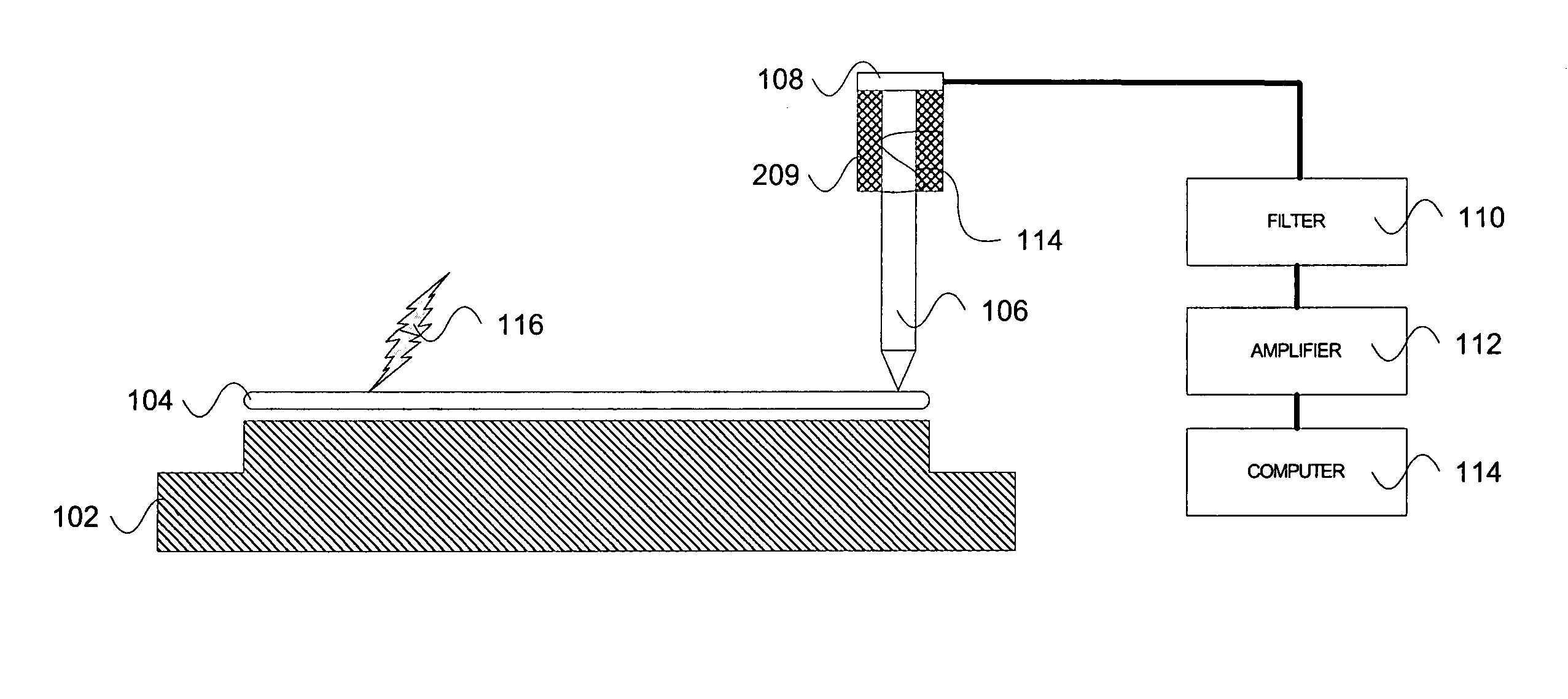
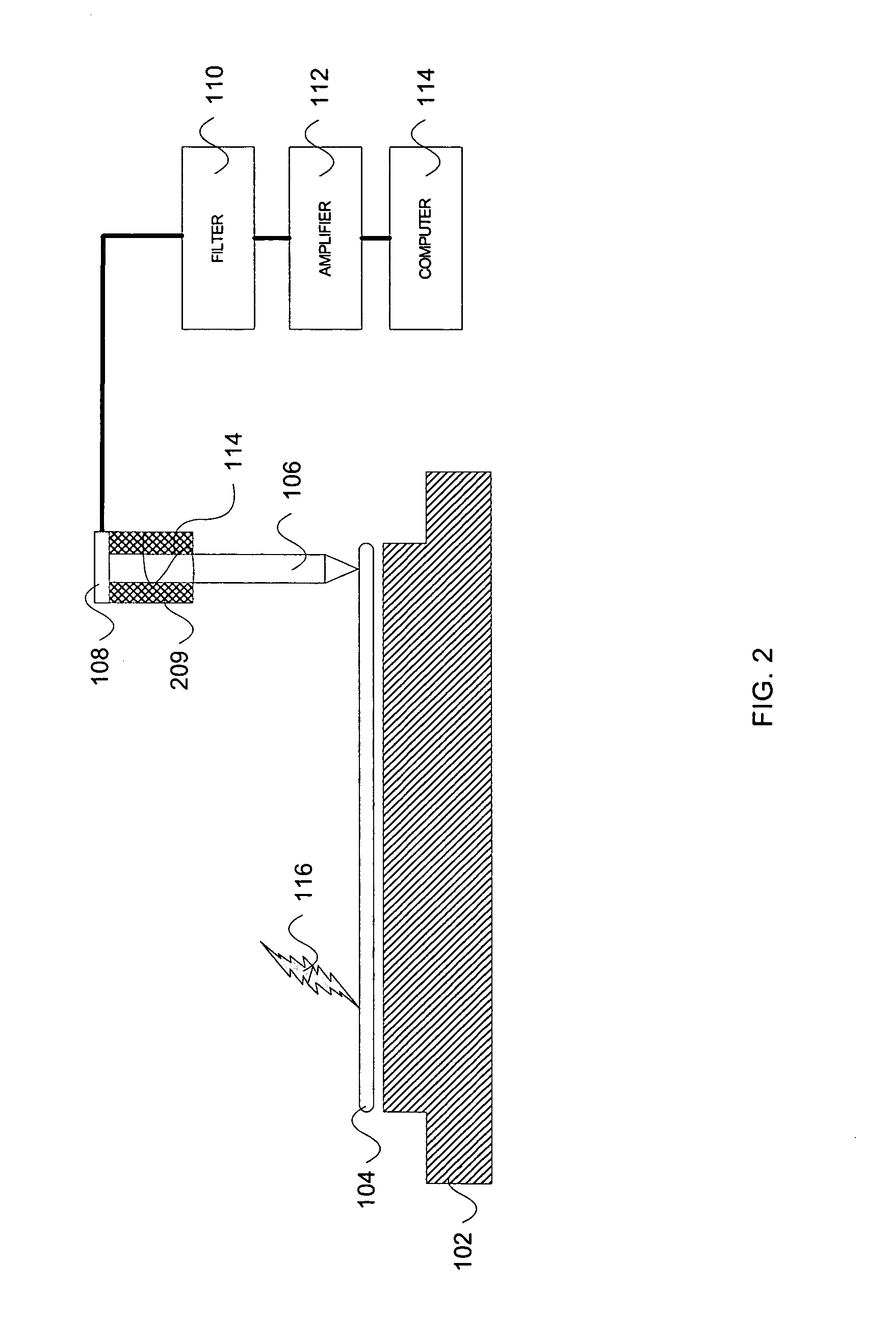
[0021]While not wishing to be bound by theory, the inventor believes that the characteristic vibration caused by an arc event, together with subsequent vibrations caused by that arc event on a substrate, can be measured in order to determine in-situ the occurrence of the arc event. That is, the frequency of the vibration signal caused by the arc may be easily distinguishable, and hence iso...


PUM

PropertyMeasurementUnit
Resilienceaaaaaaaaaa

Abstract

In a plasma processing system, a method for detecting an arc event on a substrate in a plasma chamber having a chuck is disclosed. The method includes positioning a substrate on the chuck. The method also includes providing a vibration-sensing arrangement in the plasma chamber, the vibration-sensing arrangement being configured for measuring arc-induced vibrations on the substrate, the arc-induced vibrations being generated when an arc strikes the substrate during plasma processing of the substrate in the plasma processing chamber.

Description

BACKGROUND OF THE INVENTION[0001]The present invention relates in general to substrate manufacturing technologies and in particular to apparatus and methods for the detection of an arc in a plasma processing system.[0002]In the processing of a substrate, e.g., a semiconductor substrate or a glass panel such as one used in flat panel display manufacturing, plasma is often employed. The semiconductor or glass substrate is processed in a series of steps in which materials are deposited and materials are selectively removed using plasma processes A layer of particular material is deposited on the substrate, often using plasma to enhance the deposition process. Subsequently, the layer is patterned with a polymer mask using photolithography. The substrate is then placed in a plasma processing chamber on a substrate support structure comprising a mono-polar or bi-polar electrode, called a chuck or pedestal. Appropriate etchant gases then flow into the chamber and energized to form a plasma...

Claims


Application Information

Patent Timeline
IPC IPC(8): G01H1/12G01N29/14
CPCH01J37/32935H01J2237/0206
Inventor PIRKLE, DAVID
Owner LAM RES CORP
Learn More