Magnetic memory with spin-polarized current writing, using amorphous ferromagnetic alloys, writing method for same

a writing method and magnetic memory technology, applied in the field of magnetic memories, can solve the problems of limiting integration possibilities, aging problems of ferroelectric-based memories, and risk of never writing into the selected memory poin

Inactive Publication Date: 2008-02-19
CENT NAT DE LA RECHERCHE SCI
View PDF7 Cites 33 Cited by
  • Summary
  • Abstract
  • Description
  • Claims
  • Application Information

AI Technical Summary

Problems solved by technology

Further, ferroelectric-based memories (FRAM) exhibit serious aging problems.
Indeed, the fact for the memory elements to be series-connected along each line limits integration possibilities, since the signal becomes lower and lower as the number of elements increases.
If the switching field distribution function for all memory points is wide (indeed, it is not uniform due to manufacturing constraints), the magnetic field on the selected memory point must be greater than the highest switching field of said distribution function, at the risk of incidentally switching certain memory points located on the corresponding line and / or column, having its switching field, located in the low part of the distribution, smaller than the magnetic field generated by the line or column alone.
Conversely, if it is desired to ensure that no memory point is written into by a line or a column alone, the write current must be limited to never exceed for these memory points the magnetic field corresponding to the low part of the distribution, at the risk of never writing into the selected memory point at the intersection of said lines and columns, if its switching field is in the high part of the distribution.
In other words, this architecture with a magnetic field selection by means of conductor lines and columns may easily result in write addressing errors.
In particular, the transistor control line must be offset from the lower current line (required for the writing), which minimizes integration possibilities.
The writing by a spin-polarized current being, by nature, limited to one memory point, since only the memory point having its transistor in saturated or “ON” mode conducts the write current, addressing errors are intrinsically impossible.
Unfortunately, this architecture still has up to now a serious limitation.
At the switching field, this precession is such that the magnetization of layer (40) is almost perpendicular to the layer plane, which is all the more difficult as the demagnetizing field is large.

Method used


Image

  • Magnetic memory with spin-polarized current writing, using amorphous ferromagnetic alloys, writing method for same
  • Magnetic memory with spin-polarized current writing, using amorphous ferromagnetic alloys, writing method for same
  • Magnetic memory with spin-polarized current writing, using amorphous ferromagnetic alloys, writing method for same

Examples


Embodiment Construction

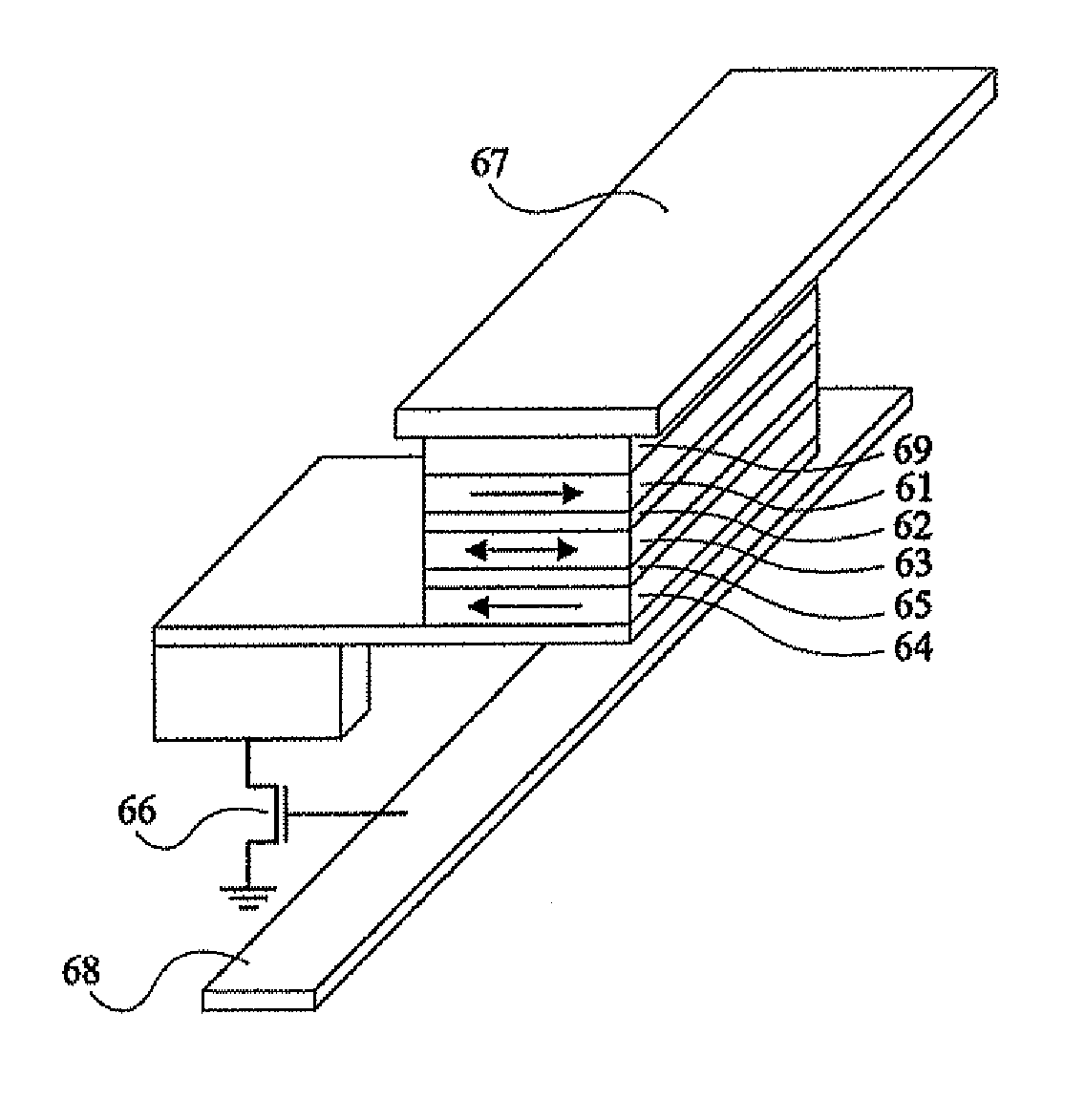
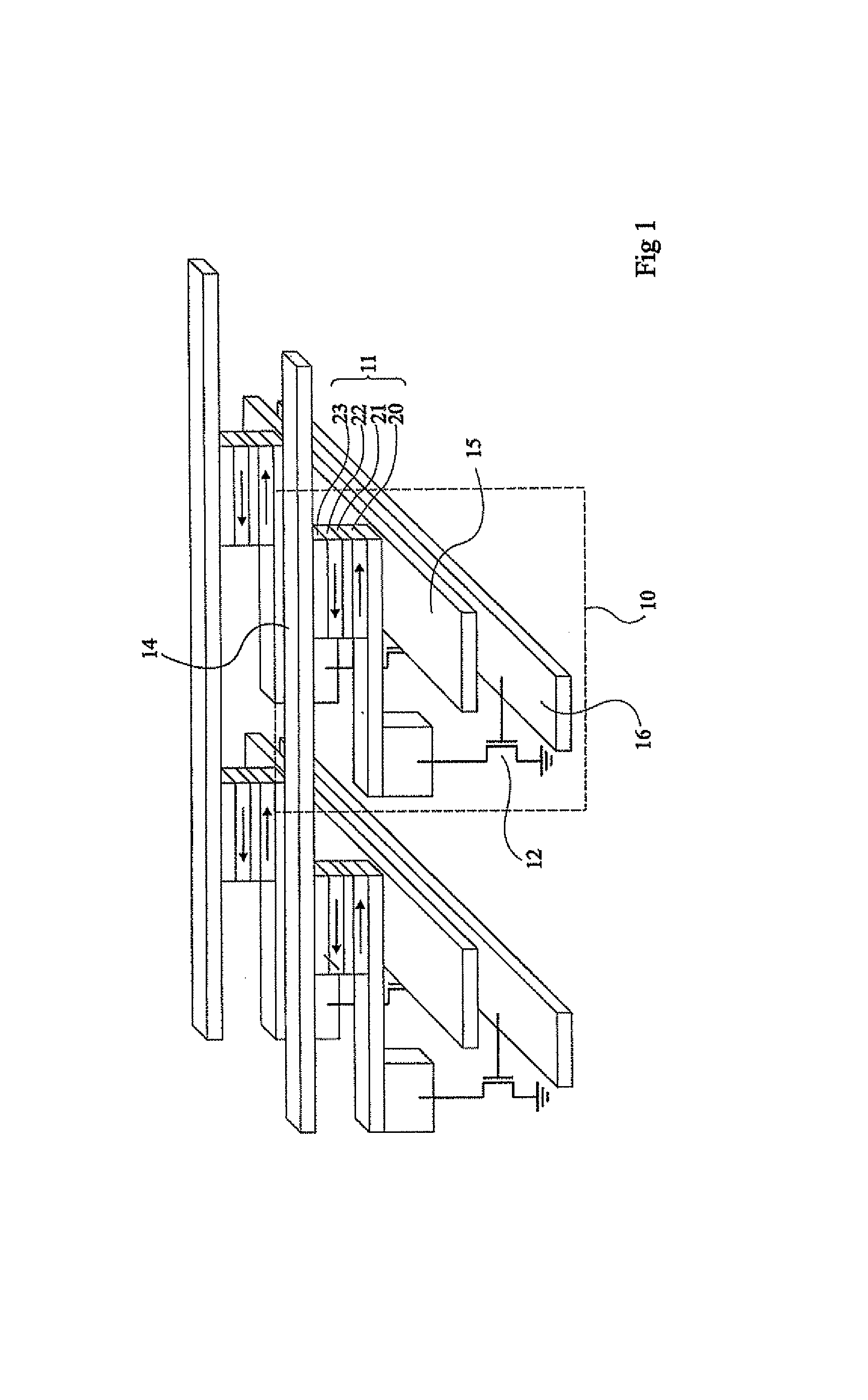
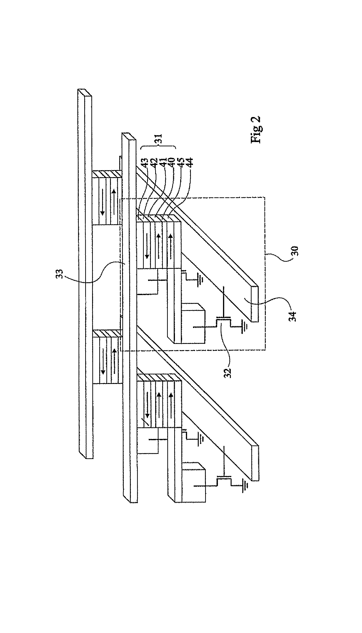
[0038]As briefly reminded hereafter, the operation of the memory according to the present invention rests on the use of FAA materials and of the specific properties associated therewith. As can be seen in FIG. 3a, macroscopic magnetization (50) of a layer (55) of an FAA can be resolved into two contributions, one contribution due to rare earth atom sub-lattice (51) and one contribution due to transition metal atom sub-lattice (52). Schematically, macroscopic magnetization (50) results from the vectorial sum of the two sub-lattices (51) and (52).

[0039]Further, the magnetizations of rare earth lattice (51) and of transition metal sub-lattice (52) are strongly coupled together, resulting in a joint behavior upon switching of macroscopic magnetization (50) or reorientation by a selective excitation of one of sub-lattices (51) and (52).

[0040]Further, when the chemical nature and the relative composition of the rare earth and of the transition metal are judiciously selected, the magnetic ...


PUM

PropertyMeasurementUnit
sizeaaaaaaaaaa
breakdown voltagesaaaaaaaaaa
magnetizationaaaaaaaaaa

Abstract

The invention concerns a magnetic memory, whereof each memory point consists of a magnetic tunnel junction (60), comprising: a magnetic layer, called trapped layer (61), whereof the magnetization is rigid; a magnetic layer, called free layer (63), whereof the magnetization may be inverse; and insulating layer (62), interposed between the free layer (73) and the trapped layer (71) and respectively in contact with said two layers. The free layer (63) is made with an amorphous or nanocrytallized alloy based on rare earth or a transition metal, the magnetic order of said alloy being of the ferromagnetic type, said free layer having a substantially planar magnetization.

Description

[0001]This application claims priority of the earlier filing date, under 35 U.S.C. 119, of the commonly owned PCT-based patent application, filing number PCT / FRO2 / 03210, filed on Sep. 19, 2002, which claims priority of French Application No. 01 / 12124 filed on Sep. 20, 2001.TECHNICAL FIELD[0002]The present invention relates to the field of magnetic memories, and especially of non-volatile random access magnetic memories enabling storage and reading of data into and from electronic systems. More specifically, it relates to magnetic random access memories, called M-RAMs, formed of a magnetic tunnel junction.STATE OF THE ART[0003]Memories based on the charge state of a capacitor (DRAM, SRAM, FLASH) become more and more sensitive to ionizing radiations (such as, for example, cosmic rays) as the dimension of elementary transistors becomes smaller. Further, ferroelectric-based memories (FRAM) exhibit serious aging problems. Recent developments in the magneto-electronic field have enabled d...

Claims


Application Information

Patent Timeline
Patent Type & Authority Patents(United States)
IPC IPC(8): H01L29/82H01L43/00G11C11/15G11C11/16H01F10/32H01L21/8246H01L27/105H01L43/08
CPCB82Y25/00G11C11/16H01F10/3204H01F10/329H01L27/226H01L43/10H01F10/3286H01F10/3268G11C11/1675G11C11/161H10B61/20H10N50/85G11C11/15
Inventor NOZIERES, JEAN-PIERRERANNO, LAURENTCONRAUX, YANN
Owner CENT NAT DE LA RECHERCHE SCI
Why Eureka
Try Eureka