
Fuse structure for semiconductor integrated circuit with improved insulation film thickness uniformity and moisture resistance

a technology of integrated circuits and fuse structures, which is applied in the field of fuse structures for semiconductor integrated circuits, can solve the problems of insufficient laser energy fuse cannot be disconnected, etc., and achieve the effect of facilitating film thickness control over the film above the fuse, reducing the proportion of fuse disconnection fault and erroneous fuse disconnection, and improving the yield of semiconductor devices

Inactive Publication Date: 2008-01-29
RENESAS ELECTRONICS CORP
View PDF5 Cites 19 Cited by
  • Summary
  • Abstract
  • Description
  • Claims
  • Application Information

AI Technical Summary

Benefits of technology

[0014]Further, in the conventional example, the insulating film on the fuse is only the SiO2 film. Thus, moisture would enter from the exterior through the opening provided above the fuse. Due to this moisture, a change in the characteristics or corrosion of the copper wiring will occur. When a Low-k film, which has a dielectric constant lower than the silicon oxide film, is in a layer below the fuse and when the moisture enters into the Low-k film, the interconnect capacitance of the Low-k film will increase. Deterioration in the long-term reliability of the semiconductor device might be brought about.
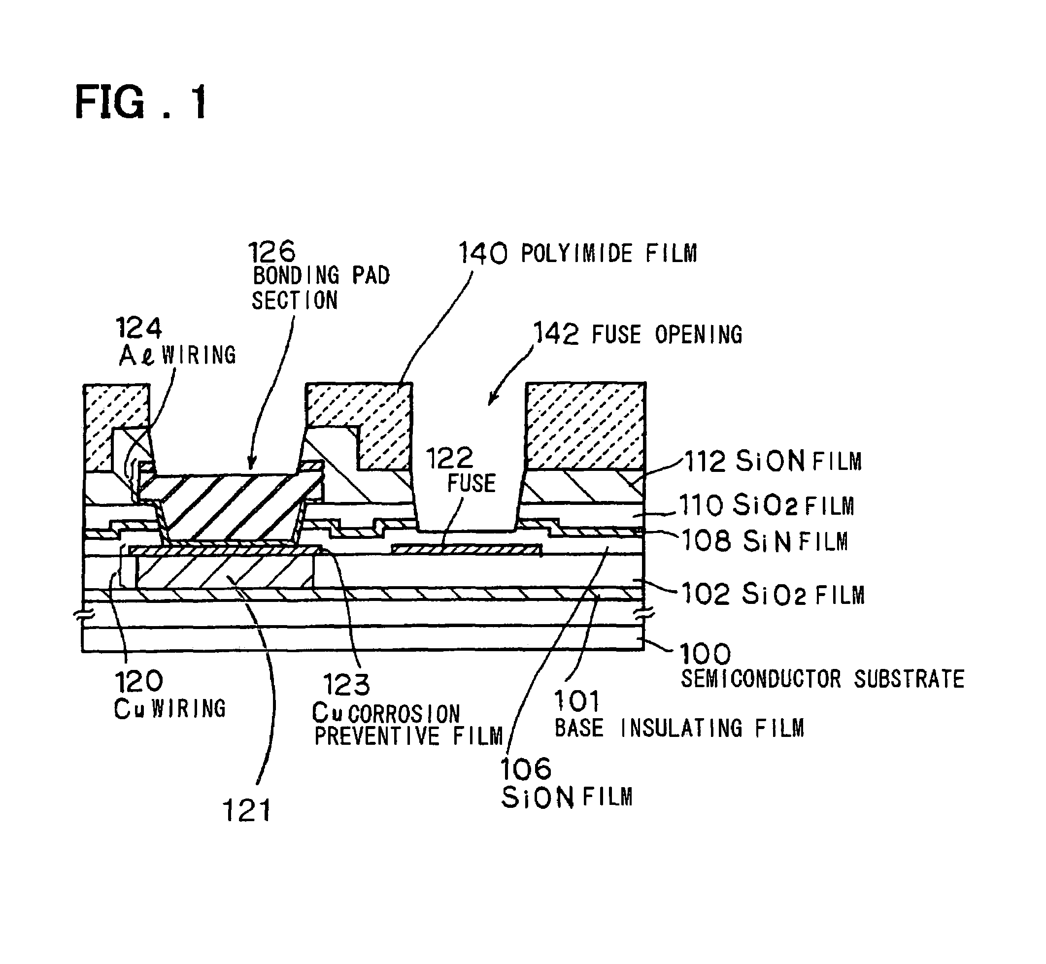
[0052]Further, in the semiconductor device of the present invention, the SiON film invariably covers the fuse (or fuses) including the opening provided above the fuse for laser irradiation. Thus, entry of the moisture from the exterior is prevented. For this reason, corrosion and change in the characteristics of the wiring are prevented. Further, even if a Low-k film of which the interconnect capacitance would be increased if the moisture enters thereinto is employed as the interlayer insulating film, entry of the moisture into the Low-k film is prevented. The reliability of the wiring is therefore markedly improved, compared with the manufacturing method of the conventional art. Thus, the reliability of the semiconductor device is improved.

Problems solved by technology

On the contrary, if the film thickness of the insulating film on the fuse becomes thicker than the set value, a problem arises that the energy of the laser becomes insufficient, so that the fuse cannot be disconnected.
For this reason, when the film thickness of the insulating film on the fuse varies even if the irradiating conditions of the laser are controlled to be the same each time the fuse is disconnected, a “disconnection fault” in which the fuse cannot be disconnected, or “erroneous disconnection” of disconnecting even an adjacent fuse tends to occur.
Due to this moisture, a change in the characteristics or corrosion of the copper wiring will occur.

Method used


Image

  • Fuse structure for semiconductor integrated circuit with improved insulation film thickness uniformity and moisture resistance
  • Fuse structure for semiconductor integrated circuit with improved insulation film thickness uniformity and moisture resistance
  • Fuse structure for semiconductor integrated circuit with improved insulation film thickness uniformity and moisture resistance

Examples


second embodiment

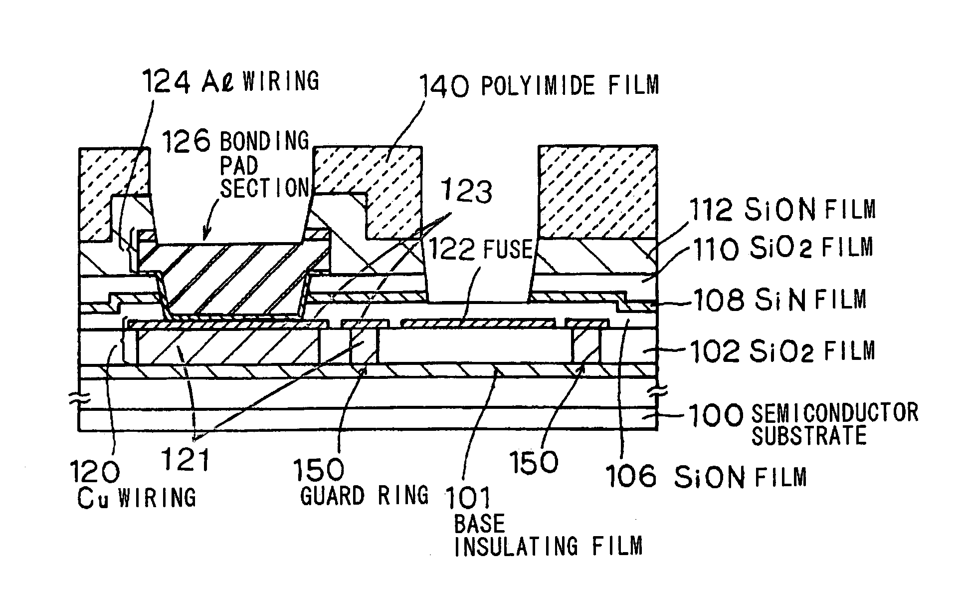
[0084]In this embodiment, a guard ring is provided for a layer underlying a region in which the fuse 122 (or fuses) is (are) formed in a configuration shown in the first embodiment so as to prevent entry of moisture after disconnection of the fuse.

[0085]A configuration of this embodiment will be described. Incidentally, same reference characters are assigned to the same configurations as in the first embodiment, and their detailed description will be omitted.

[0086]FIG. 4A is a schematic sectional view showing an example of the configuration of this embodiment. FIG. 4B is a schematic plan view showing layer patterns of the Cu wiring 120 and the fuses 122, and a sectional view along a line section X-X′ corresponds to FIG. 4A.

[0087]As shown in FIGS. 4A and 4B, a guard ring 150 surrounding the planar pattern region of the fuses 122 is formed in the SiO2 film 102 underlying the fuses 122, using the Cu wiring. More specifically, the guard ring 150 is formed, being embedded in the SiO2 fil...


PUM


Abstract

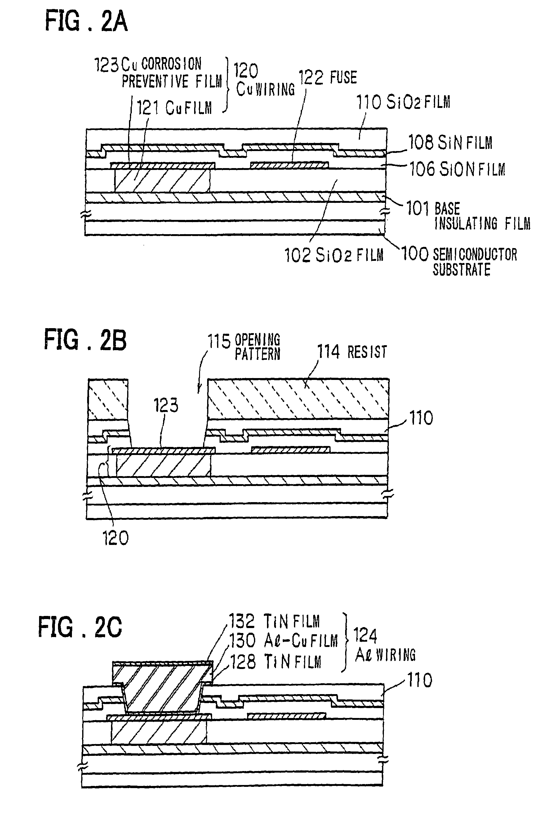
When the film thickness of an insulating film on a fuse connected to a circuit is not uniform within a wafer surface, there was a problem that disconnection of the fuse might become insufficient due to the insufficient intensity of a laser or disconnection of even an adjacent fuse due to excessive laser irradiation might occur. Further, a problem also occurred that after disconnection of the fuse, moisture entered from exterior through the region in which the fuse has been disconnected, so that the quality of a film underlying the fuse was adversely affected. After a SiON film, a SiN film, and a SiO2 film have been formed to cover the fuse in this stated order, etching is performed to the SiN film, which is an etching stopper film. The SiON film having a uniform and desired film thickness is thereby formed on the fuse.

Description

FIELD OF THE INVENTION[0001]The present invention relates to a semiconductor device including circuit elements such as a memory and logic and a manufacturing method thereof.BACKGROUND OF THE INVENTION[0002]Conventionally, some memories such as DRAMs in semiconductor devices include fuses so as to cause redundancy bits replacing defective bits to function (refer to Nonpatent Document 1, for example). The operation of the semiconductor device is checked after a wafer manufacturing process thereof, and if a defective bit is detected, a laser is irradiated onto a fuse connected to the defective bit for disconnection, so as to replace the defective bit with a redundancy bit.[0003]As the method of using fuses in the semiconductor device, there is provided a method as follows, in addition to the method in case of the memory. Assume that recording of information “1” or “0” is performed, responsive to a state where the fuse is disconnected or not. Then, by providing 128 fuses for each semico...

Claims


Application Information

Patent Timeline
Patent Type & Authority Patents(United States)
IPC IPC(8): H01L21/768H01L23/52H01L21/3205H01L21/82H01L23/00H01L23/31H01L23/485H01L23/522H01L23/525H01L23/58H01L27/10
CPCH01L23/3192H01L23/5258H01L23/564H01L23/585H01L24/03H01L24/05H01L2924/01006H01L2924/01007H01L2224/04042H01L2224/02166H01L2224/48847H01L2924/00014H01L2924/01019H01L24/45H01L2924/01005H01L2924/01004H01L2924/01002H01L2924/01013H01L2924/01014H01L2924/01015H01L2924/01022H01L2924/01029H01L2924/01033H01L2924/0105H01L2924/01051H01L2924/01078H01L2924/01082H01L2924/05042H01L2924/14H01L2924/19041H01L2924/19043H01L2924/30105H01L2924/3025H01L2224/05599H01L2224/05624H01L2224/05647H01L2224/45147H01L2224/48824H01L2924/00H01L2924/12042
Inventor SAKOH, TAKASHI
Owner RENESAS ELECTRONICS CORP
Learn More