Method for physical placement of an integrated circuit based on timing constraints

a timing constraint and integrated circuit technology, applied in the field of integrated circuits, can solve the problems of complex operation of designing an integrated circuit with millions of logic gates, non-optimal timing, and difficult timing closur

Inactive Publication Date: 2008-01-08
CISCO TECH INC
View PDF1 Cites 8 Cited by
  • Summary
  • Abstract
  • Description
  • Claims
  • Application Information

AI Technical Summary

Benefits of technology

[0014]A timing budget is a distribution of the available time for a signal to reach from a first node in a path to a second node in the path. Examples of node may include a flip-flop (FF), a logic gate, and the like. Various timing budgets can exist for various inter-block paths. An inter-block path can be a path that connects a source block and a sink block in the IC. The inter-block path further comprises at least three portions: source block portion, top-level portion, and sink block portion. The timing budget can be distributed between the top-level portion and the block portions of an inter-block path. To obtain the maximum performance from the inter-block path, timing constraints related to source and sink blocks on the inter-block path should be considered. Further, block areas of source and sink blocks and levels of logic attached to the block ports in the source and sink blocks should also be considered. The levels of logic of a block can be the maximum number of logic gates between a block port and a flip-flop stage. In an embodiment of the invention, the logic gates can be specifically non-sequential logic gates. It can be more difficult for a block with a larger area and levels of logic to fulfill the timing constraints than for a block with a smaller area and levels of logic. Therefore, the block with a larger area and levels of logic should be given more lenient timing constraints. Then the placement / synthesis tool can more easily create the optimal timing results even for the block with the large area and levels of logic.

Problems solved by technology

Designing an integrated circuit with millions of logic gates is a complex operation.
Timing closure becomes a challenging task for an IC with millions of logic gates.
When these conventional techniques are applied globally in the IC design, the timing budget allocation may not be precise and result in non-optimal timing results.
Therefore, the conventional techniques may not predict the timing performance of the individual paths precisely.
In the process of placing over-constrained paths, the placement / synthesis tool will waste time trying to meet unachievable timing constraints.
Further, the placement / synthesis tool will also work harder than necessary on a path that could negatively affect other paths.
Therefore, the task of fulfilling the timing constraints for an over-constrained path by the synthesis tool can be unnecessarily time consuming.
Therefore, if a large number of paths are under-constrained, then the synthesis tool might quit the task of creating optimal timing results pre-maturely, considering the improvements made by this task to be insignificant in the overall timing performance.
Further, while timing an inter-block path that has under-constrained block level timing constraints, the timing constraints for the block level may be satisfied but the timing constraints for the top level may not be satisfied, resulting in failing timing results for the top level.
Therefore, the timing performance of a path in the IC is not optimized due to over-constrained and under-constrained paths.
But writing the timing constraints and analyzing the timing performance manually for tens or hundreds of thousands of paths in the IC is a cumbersome task.
However, equal treatment of all bits may not result in an optimal solution since each bit may have a different level of combinational logic processing, depending on the design of the IC.
The problem with such EDA tools is that they may provide top-level timing correction only for an inter-block path, which is failing to operate according to timing constraints.
Moreover, this timing correction may only be a best-effort timing correction as it may not be able to modify the placement of certain elements in a path of the IC.
Further, these tools may not consider the slack available anywhere else in the design for timing budget allocation.
Therefore, using only existing EDA tools alone may result in non-optimal timing budget allocation and therefore non-optimal timing results.

Method used


Image

  • Method for physical placement of an integrated circuit based on timing constraints
  • Method for physical placement of an integrated circuit based on timing constraints
  • Method for physical placement of an integrated circuit based on timing constraints

Examples


Embodiment Construction

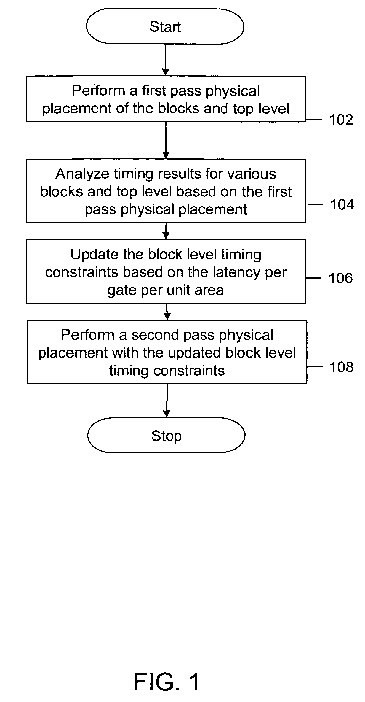
[0013]Various embodiments of the invention provide a method, a system, and an apparatus for physical placement of an integrated circuit based on timing constraints. The method involves a two-pass physical placement technique, which results in the optimal placement of all inter-block paths in the IC. After the first pass of the physical placement of the blocks and the top level, the timing results of the top level and of each block are analyzed. The method involves the computation of latency per gate per unit area (LPGA) of each block port of each block in the IC. Based on the calculated LPGA, the timing constraints of the blocks are updated. The second pass of physical placement is performed, based on the updated timing constraints.

[0014]A timing budget is a distribution of the available time for a signal to reach from a first node in a path to a second node in the path. Examples of node may include a flip-flop (FF), a logic gate, and the like. Various timing budgets can exist for v...


PUM


Abstract

A method, system, apparatus, and machine-readable medium for physical placement of an integrated circuit based on the timing constraints are provided. The method involves a two-pass physical placement technique. After the first pass of the physical placements of the blocks and the top level, the timing results of the top level and of each block are analyzed. The method involves the computation of latency per gate per unit area (LPGA) of the block ports of each block. Based on the calculated LPGA, the timing constraints of the blocks are updated. The second pass of physical placement is performed, based on the updated timing constraints.

Description

BACKGROUND OF THE INVENTION[0001]1. Field of Invention[0002]Embodiments of the invention relate in general to Integrated Circuits (ICs). More specifically, the embodiments of the invention relate to methods and systems for physical placement of an integrated circuit based on the timing constraints of the integrated circuit.[0003]2. Description of the Background Art[0004]Designing an integrated circuit with millions of logic gates is a complex operation. While performing physical placement of an IC, timing closure is performed iteratively to obtain optimal timing performance. Timing closure can be defined as a process by which timing results on all paths in the IC are met according to standards as defined by the IC technology used and the product specifications. Timing closure becomes a challenging task for an IC with millions of logic gates. A part of the timing closure task involves timing budget allocation on various paths in the IC and further satisfying these timing budgets. A t...

Claims


Application Information

Patent Timeline
Patent Type & Authority Patents(United States)
IPC IPC(8): G06F17/50
CPCG06F17/5031G06F17/5072G06F30/3312G06F30/392
Inventor CADIEUX, STEPHEN
Owner CISCO TECH INC
Why Eureka
Try Eureka