
Semiconductor memory device for a low voltage operation

a memory device and low-voltage technology, applied in the direction of information storage, static storage, digital storage, etc., can solve the problems of reducing the consumption power of transistors manufactured compared to before, difficult to reduce process technology further, and more rapid operation speed, so as to achieve the same operation speed and reduce leakage current

Inactive Publication Date: 2007-11-13
SK HYNIX INC
View PDF12 Cites 4 Cited by
  • Summary
  • Abstract
  • Description
  • Claims
  • Application Information

AI Technical Summary

Benefits of technology

[0073]It is, therefore, a primary object of the present invention to provide to a semiconductor memory device that is capable of maintaining a same operation speed, without a use of high voltage, even when a driving voltage is low (e.g., 1.0V or less). In particular, the present invention provides a semiconductor memory device capable of reducing a leakage current in a bit line sense amp unit at a low voltage.

Problems solved by technology

In other words, improving the process technology results in a decrease in consumption power of transistor manufactured compared to before and also more rapid operation speed than before, upon a supply of the same voltage.
However, it is very difficult to decrease the process technology further as before, under 100 nm.
Furthermore, under the situation that the required supply voltage is low to 1.5V below 2.0V, so far as 1.0V, it is very hard to maintain the operation speed as before, by the decrease of the process technology merely.
Moreover, if the level of the supply voltage supplied to the memory device is lower than a fixed level, then an operation margin of MOS transistor constituting the memory device is very small, thus making it to be not operated at the required operation speed and also lowering the reliability of operation.
Thus, decreasing the driving voltage of the memory device below the constant level is very hard under the existing technology.
Further, if the manufacturing technology of the memory device is very improved, a space between the gate polarity of MOS transistor constituting each unit cell and its adjacent bit lines becomes very small, thus incurring a leakage current between the gate polarity and the bit lines.
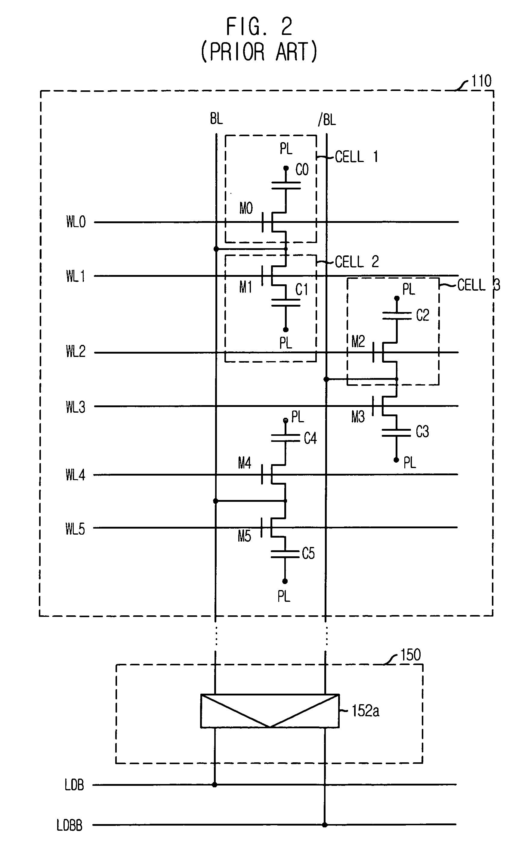
Due to the decrease in the process technology of the semiconductor memory device, an interval A between the gate polarity 13 and the bit line 17 becomes narrow gradually, making sufficient isolation difficult.
As the technology develops, it is very important issue to operate the memory device at low power.
But, as long as there occurs the bleed current, such semiconductor memory device may be not employed in a system, even under an absence of the operation problem.
Such idea merely reduces the bleed current somewhat but does not present any fundamental solution.
Another problem is that there is leakage current between the bit line sense amp and cell arrays that are not connected thereto.

Method used


Image

  • Semiconductor memory device for a low voltage operation
  • Semiconductor memory device for a low voltage operation
  • Semiconductor memory device for a low voltage operation

Examples


Embodiment Construction

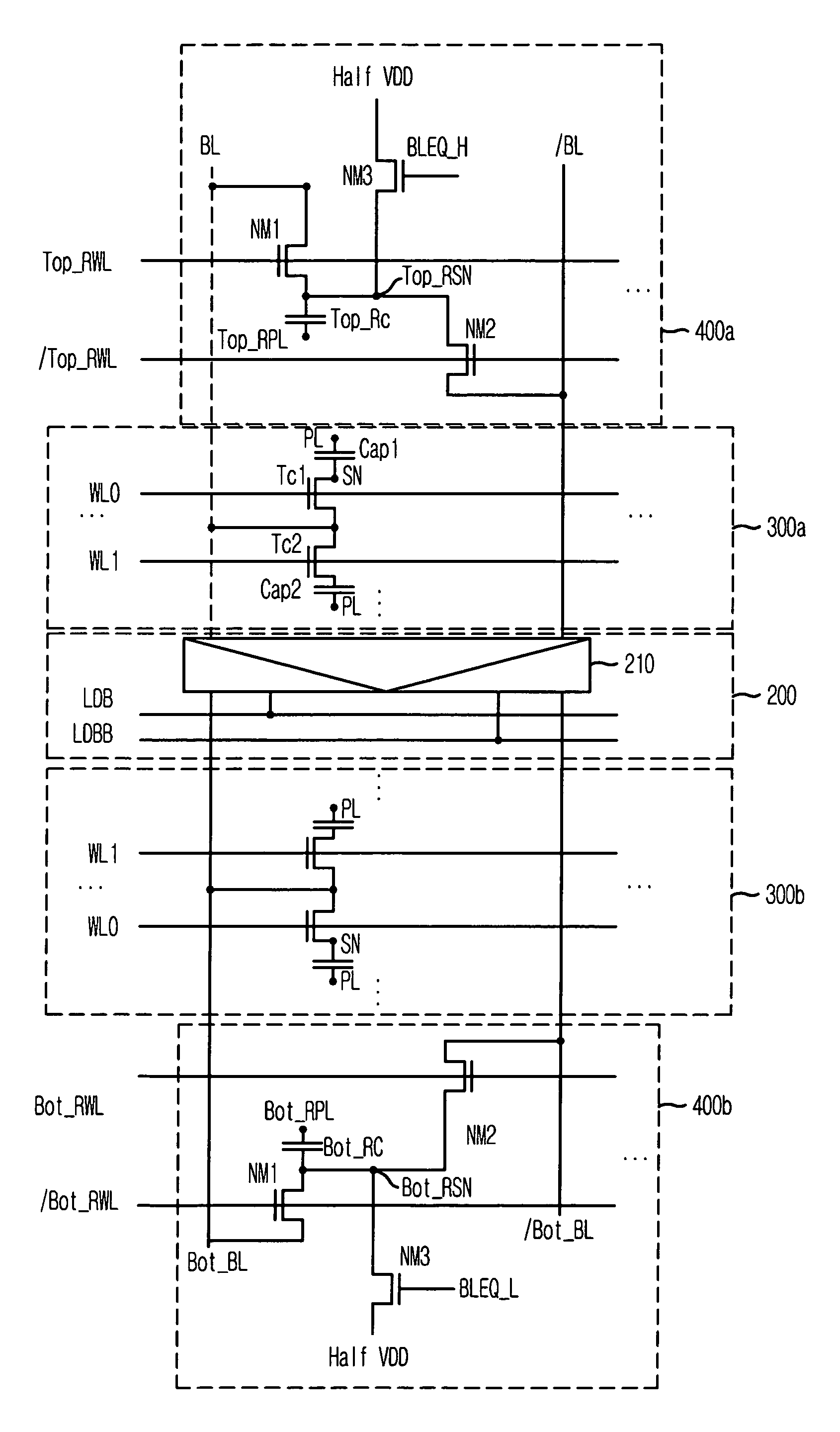
[0085]In accordance with one aspect of the present invention, there is provided a semiconductor memory device with a folded bit line structure, which is operative by an input of a supply voltage and a ground voltage, comprising: a first cell array for applying a data signal onto a first bit line or a first bit line bar; a first reference cell block for applying a reference signal onto the first bit line bar when the data signal is inputted onto the first bit line, or the reference signal onto the first bit line bar when the data signal is inputted onto the first bit line bar; a second cell array for applying the data signal onto a second bit line or a second bit line bar; a second reference cell block for applying the reference signal onto the second bit line bar when the data signal is inputted onto the second bit line, or the reference signal onto the second bit line bar when the data signal is inputted onto the second bit line bar; and a bit line sense amp for sensing and amplify...


PUM


Abstract

A semiconductor memory includes first and second cell arrays for applying a data signal onto pairs of first bit lines and second bit lines, respectively, first and second reference cell blocks each of which applies a reference signal onto a corresponding bit line bar or a corresponding bit line when the data signal is inputted to the corresponding bit line or the corresponding bit line bar, and a sense amp for sensing and amplifying a difference of data signals applied onto one pair of bit lines connected thereto of the pairs of first and second bit lines, wherein each bit line maintains a floating state without an input of an extra pre-charge voltage upon a pre-charge operation, and the other pair of bit lines disconnected to the sense amp are pre-charged with the reference signal by the corresponding reference cell block.

Description

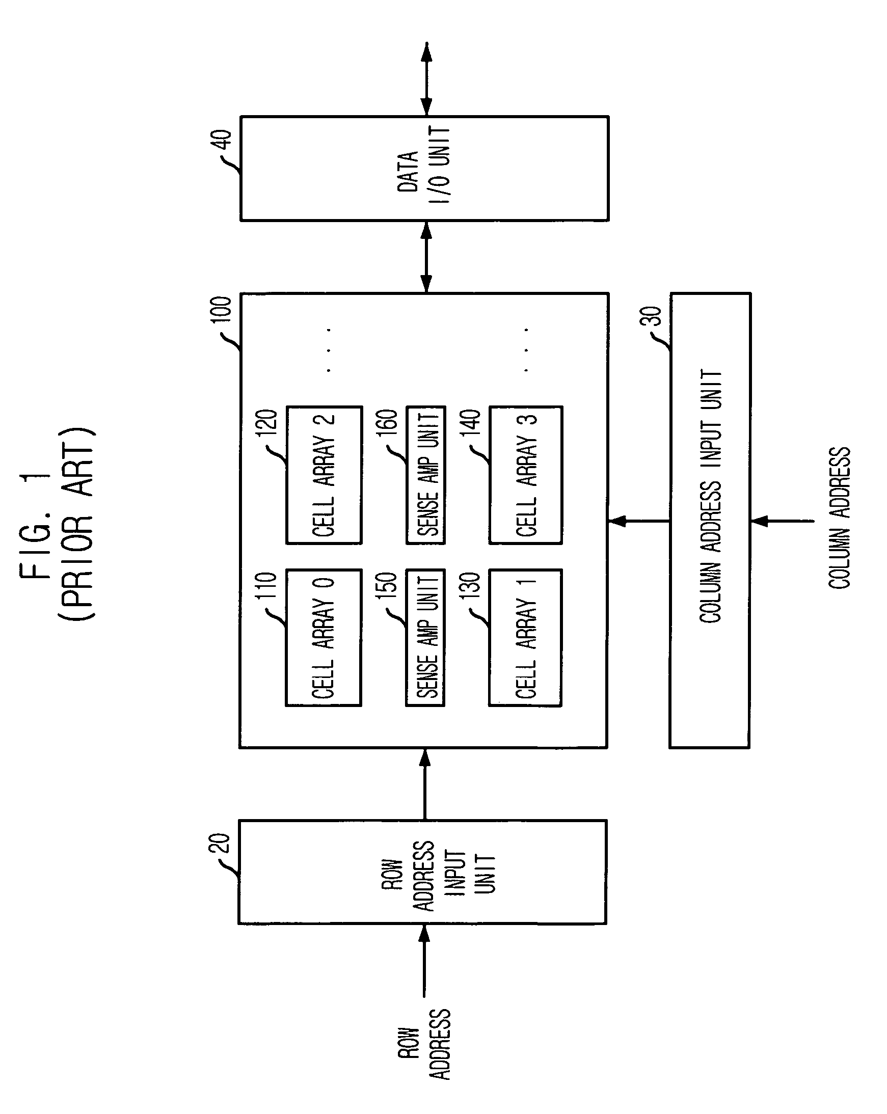
FIELD OF THE INVENTION[0001]The present invention relates to a semiconductor memory device; and, more particularly, to a semiconductor memory device that is capable of operating efficiently when a supply voltage to the device is low.BACKGROUND OF THE INVENTION[0002]FIG. 1 shows a block diagram illustrating a configuration of a conventional semiconductor memory device.[0003]Referring to FIG. 1, the conventional semiconductor memory device comprises a row address input unit 20 for inputting and decoding a row address to output decoded data, a column address input unit 30 for inputting and decoding a column address to provide decoded data, a cell region unit 100 having plural cell arrays 110 to 140 with unit cells for outputting the data from the row address input unit 20 and the column address input unit 30, and a data input / output (I / O) unit 40 for transferring the data from the cell region unit 100 to the outside, or delivering data from the outside to the cell region unit 100.[0004...

Claims


Application Information

Patent Timeline
Patent Type & Authority Patents(United States)
IPC IPC(8): G11C7/00
CPCG11C11/4091G11C11/4097G11C2207/005G11C7/062G11C7/12G11C11/4094G11C2207/2227G11C2207/002
Inventor KANG, HEE-BOKAHN, JIN-HONG
Owner SK HYNIX INC
Learn More