
Differential output driver and semiconductor device having the same

a technology of output signal and output signal, which is applied in the direction of logic circuit coupling/interface arrangement, pulse technique, separation process, etc., can solve the problems of degrading signal characteristics, output signal and inverted output signal having voltage differences outside the desired range, etc., to improve signal characteristics of differential output signals and reduce swing width differences.

Inactive Publication Date: 2007-10-30
SAMSUNG ELECTRONICS CO LTD
View PDF7 Cites 30 Cited by
  • Summary
  • Abstract
  • Description
  • Claims
  • Application Information

AI Technical Summary

Benefits of technology

The invention provides a differential output driver that can improve the signal quality of two differential output signals by reducing the difference in swing width between them, even when the values of elements change due to changes in process, voltage, or temperature. The driver includes a differential output portion with first and second on-die termination resistors, a first driver to generate the inverted output signal, and a second driver to generate the output signal. Additionally, an inverted output signal drive variable portion and an output signal drive variable portion are connected in parallel to the first and second drivers, respectively, to vary their driving capabilities in response to control signals. A controller is also included to detect voltage differences between a reference voltage and the inverted output signal and the output signal, and generate the control signals based on the detected errors.

Problems solved by technology

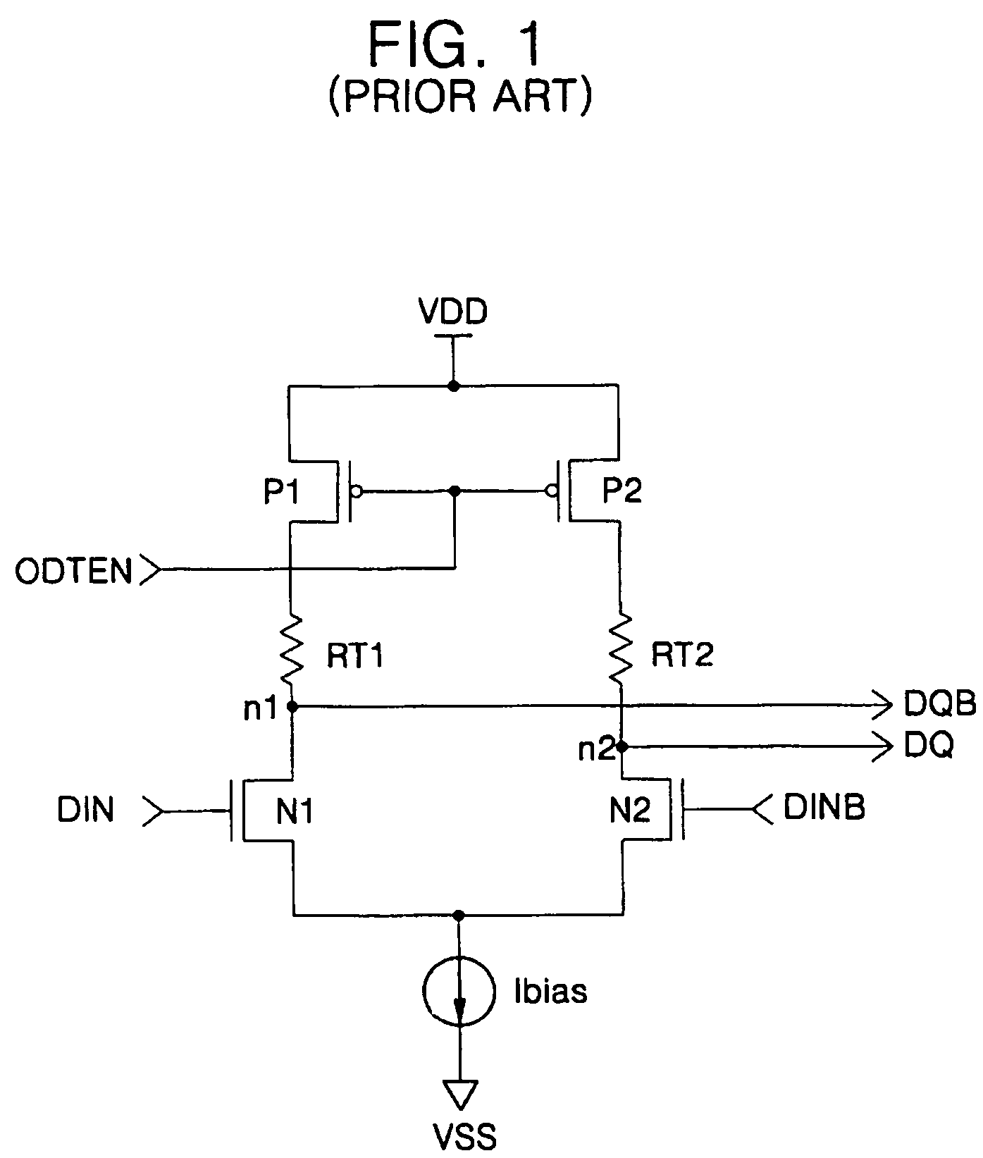
However, values of elements constituting the differential output driver vary due to changes in process, voltage, or temperature, resulting in the output signal and the inverted output signal having a voltage difference outside of a desired range.
Consequently, the signal width of the pair of different output signals DQ and DQB becomes narrower, which degrades signal characteristics.

Method used


Image

  • Differential output driver and semiconductor device having the same
  • Differential output driver and semiconductor device having the same
  • Differential output driver and semiconductor device having the same

Examples


Embodiment Construction

[0020]Hereinafter, a differential output driver and a semiconductor device having the same will be described with reference to the accompanying drawings.

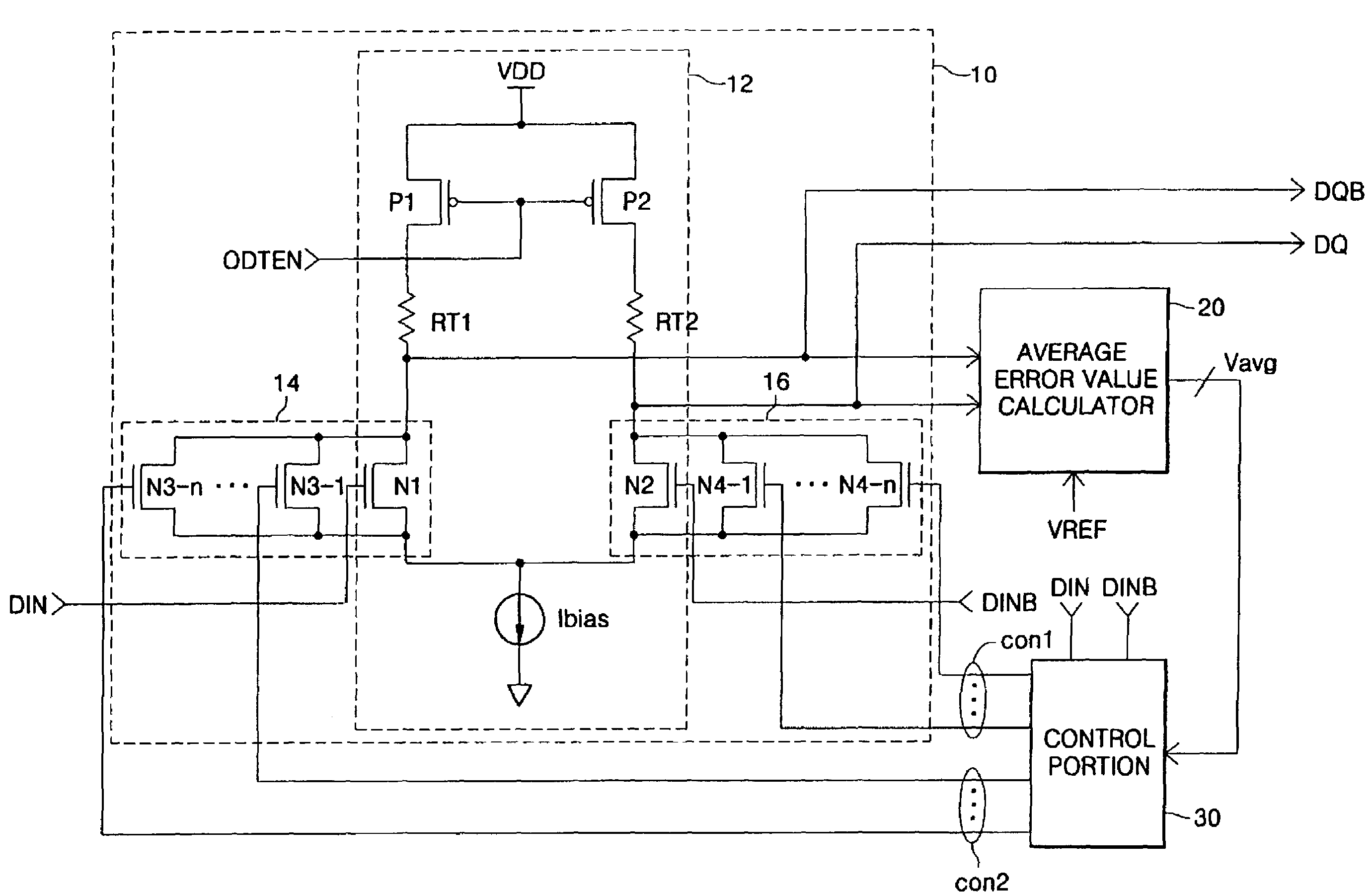
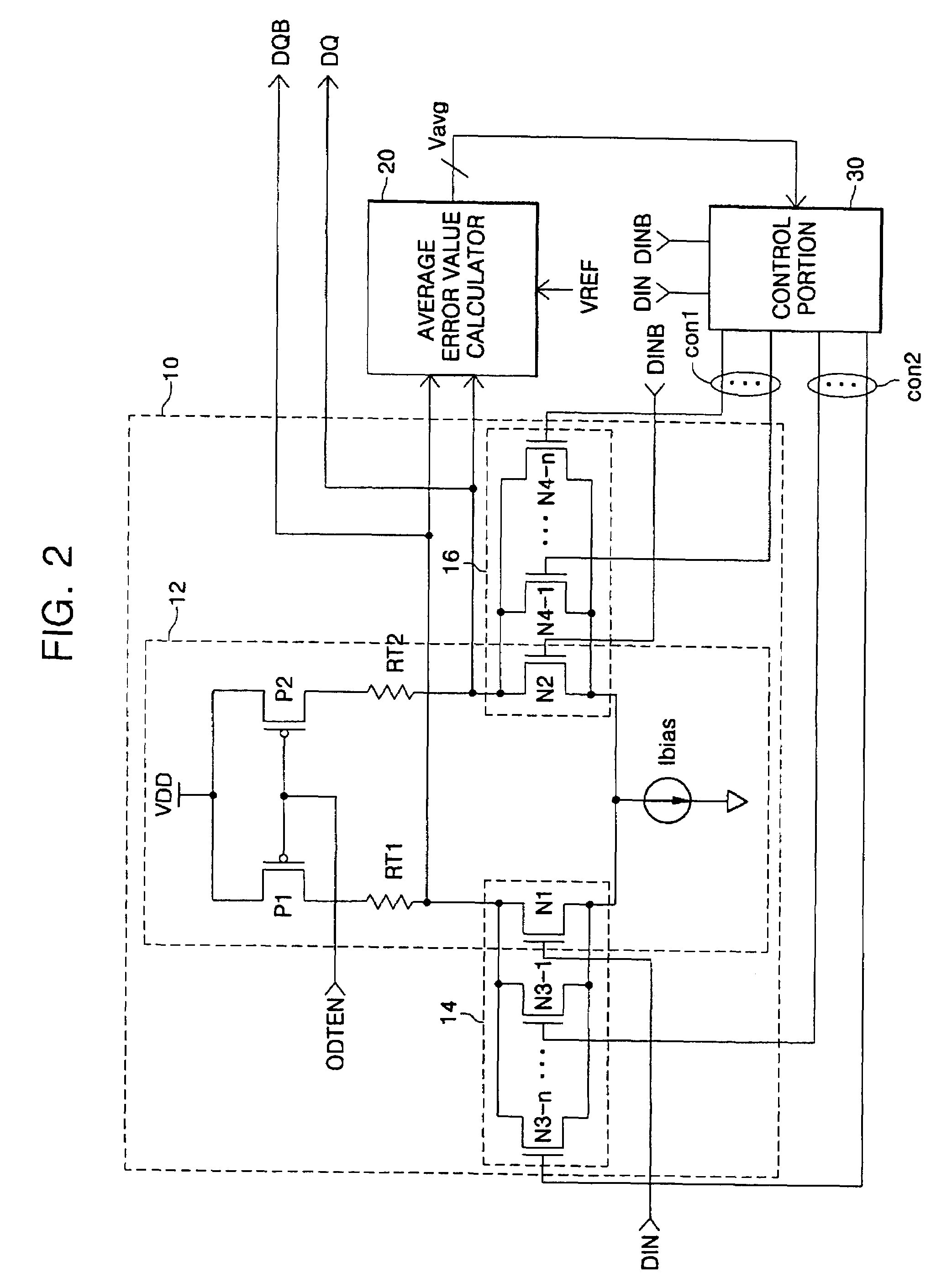
[0021]FIG. 2 is a diagram illustrating the structure of a differential output driver in accordance with an embodiment of the present invention. The embodiment illustrated in FIG. 2 includes a driver 10, an average error value calculator 20, and a control portion 30. The driver 10 has a differential output portion 12, an inverted output signal drive variable portion 14, and an output signal drive variable portion 16. The differential output portion 12 includes PMOS transistors P1 and P2, termination resistors RT1 and RT2, and NMOS transistors N1 and N2. The inverted output signal drive variable portion 14 is composed of NMOS transistors N3-1 to N3-n. The output signal drive variable portion 16 is composed of NMOS transistors N4-1 to N4-n.

[0022]The function of the differential output driver shown in FIG. 2 is now described below.

[002...


PUM

PropertyMeasurementUnit
voltageaaaaaaaaaa
frequencyaaaaaaaaaa
voltage differenceaaaaaaaaaa

Abstract

An embodiment of a differential output driver includes a driver to generate an inverted output signal in response to an input signal and a first control signal, and to further generate an output signal in response to an inverted input signal and a second control signal. The differential output driver also includes a controller to generate the first control signal and the second control signal in response to detecting a voltage difference between a first detected voltage difference between a reference voltage and the output signal, and a second detected voltage difference between the reference voltage and the inverted output signal.

Description

CROSS-REFERENCE TO RELATED APPLICATION[0001]This application claims the benefit of Korean Patent Application No. 10-2005-0005149, filed Jan. 19, 2005, the disclosure of which is hereby incorporated herein by reference in its entirety.BACKGROUND OF THE INVENTION[0002]1. Field of the Invention[0003]The present invention relates to an output driver, and more particularly, to a differential output driver and a semiconductor device having the same, in which a differential input signal is received and a differential output signal is generated.[0004]2. Description of the Related Art[0005]A differential output driver of a conventional semiconductor device receives a differential input signal and generates an output signal and an inverted output signal which have a voltage difference within a constant range. However, values of elements constituting the differential output driver vary due to changes in process, voltage, or temperature, resulting in the output signal and the inverted output si...

Claims


Application Information

Patent Timeline
Patent Type & Authority Patents(United States)
IPC IPC(8): H03K19/0175H03K19/094
CPCH03F3/211H03F3/45183H03F3/45475H03F3/45744H03F3/45928H03K19/018528H03K19/00384H03F3/45968H03F2200/447H03F2203/45286H03F2203/45371B01D21/245C02F1/52
Inventor BYUN, GYUNG-SUBAE, IL-MAN
Owner SAMSUNG ELECTRONICS CO LTD
Learn More