
Apparatus and methods for searching through and analyzing defect images and wafer maps

Active Publication Date: 2007-10-16
KLA TENCOR CORP
View PDF31 Cites 47 Cited by
  • Summary
  • Abstract
  • Description
  • Claims
  • Application Information

AI Technical Summary

Benefits of technology

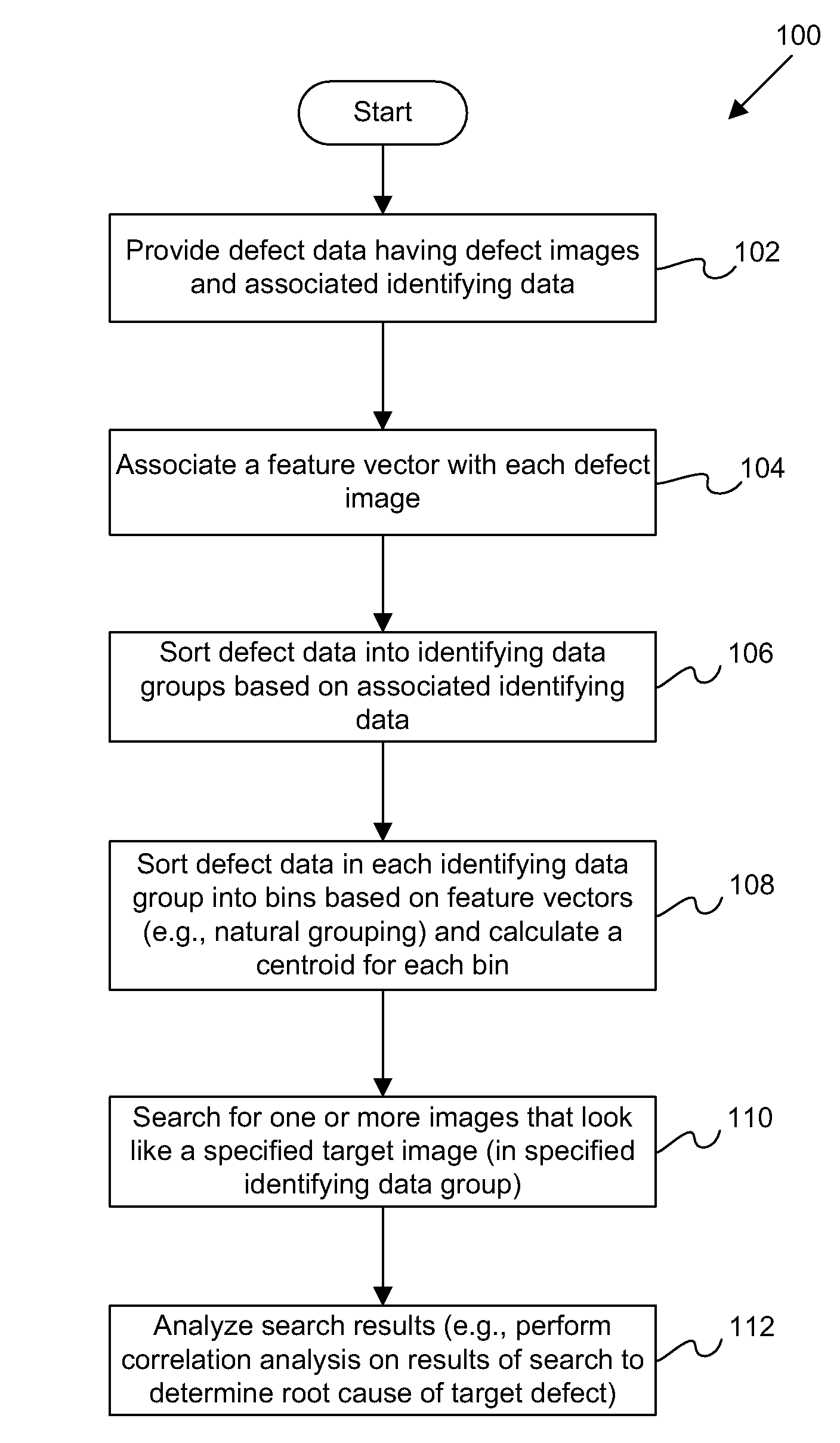
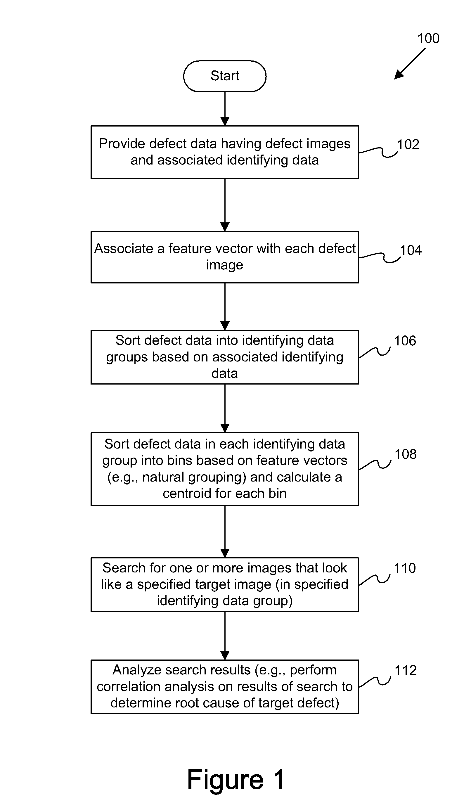
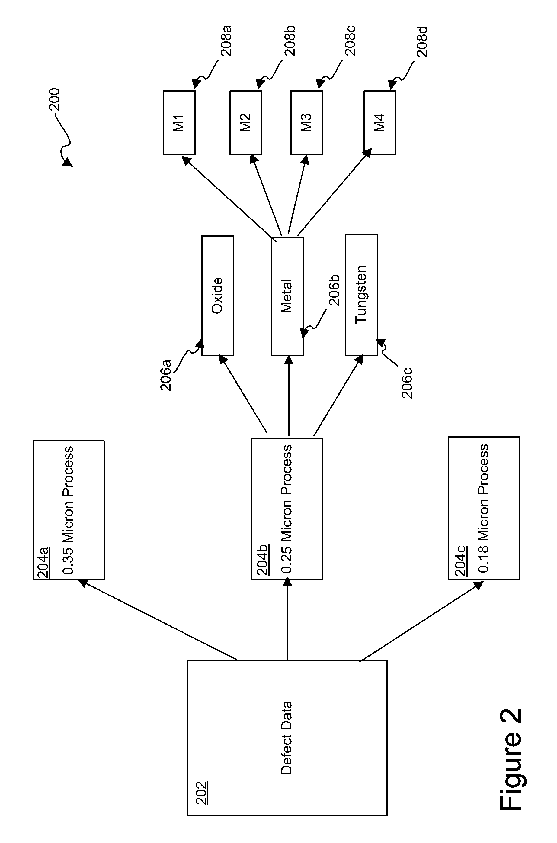
[0017]Accordingly, mechanisms are provided for automatically organizing and / or analyzing a plurality of defect images without first providing a predefined set of classified images (herein referred to as a training set). In other words, sorting is not based on a training set or predefined classification codes for such defect images. In one embodiment, the defect images each include associated identifying data, such as a fabrication identifier, lot number, wafer number, and layer identifier. Initially, the defect images are sorted according to at least a portion of the associated identifying data into a plurality of “identifying data groups” or image families. The defect data in each identifying data group is then automatically sorted according to defect appearance. That is, similar defect images are associated with a single bin and similar bins are associated with other similar bins. For example, similar bins are arranged next to each other within a graphical user interface (GUI). A representative feature vector (herein referred to as a “centroid”) is then associated with each bin. The centroid generally represents the images within the particular bin. A search for images that “look like” a specified target image may then be efficiently performed on a particular identifying data group using the centroids of each bin. The target image's feature vector is compared with the centroid of each bin that is within the same identifying data group or image family as the target image. The techniques of the present invention may also be applied to wafer maps, as well as defect images.

Problems solved by technology

Semiconductor defects may include structural flaws, residual process material and other surface contamination which occur during the production of semiconductor wafers.
Problems with this classification method include the technician's subjectivity in identifying the defect class, and the fatigue associated with the highly repetitive task of observing and classifying these defects.
While this system reduces technician fatigue and increases the number of defects that can be classified per unit time, there is presently a problem with such KDB programs providing an accurate classification.
A knowledge database generated by this method is subject to inaccuracy since human variability, introduced in the initial subjective identification of the defect type, is included in the KDB.
Moreover, present database generating methods, including direct coding, are time consuming and require a significant amount of highly trained, manpower resources.
However, if the underlying classes are inaccurately defined, the search will produce inaccurate results.
The search will also not be able to locate defects which have not been previously classified.
Since each class may have thousands of defect images, this search can take a significant amount of time.

Method used


Image

  • Apparatus and methods for searching through and analyzing defect images and wafer maps
  • Apparatus and methods for searching through and analyzing defect images and wafer maps
  • Apparatus and methods for searching through and analyzing defect images and wafer maps

Examples


Embodiment Construction

[0034]Reference will now be made in detail to a specific embodiment of the invention. An example of this embodiment is illustrated in the accompanying drawings. While the invention will be described in conjunction with this specific embodiment, it will be understood that it is not intended to limit the invention to one embodiment. On the contrary, it is intended to cover alternatives, modifications, and equivalents as may be included within the spirit and scope of the invention as defined by the appended claims. In the following description, numerous specific details are set forth in order to provide a thorough understanding of the present invention. The present invention may be practiced without some or all of these specific details. In other instances, well known process operations have not been described in detail in order not to unnecessarily obscure the present invention.

[0035]FIG. 1 is a flowchart illustrating a procedure 100 for analyzing defects in accordance with one embodi...


PUM


Abstract

Disclosed are methods and apparatus for automatically organizing and / or analyzing a plurality of defect images without first providing a predefined set of classified images (herein referred to as a training set). In other words, sorting is not based on a training set or predefined classification codes for such defect images. In one embodiment, the defect images each include associated identifying data, such as a fabrication identifier, lot number, wafer number, and layer identifier. Initially, the defect images are sorted according to at least a portion of the associated identifying data into a plurality of “identifying data groups” or image families. The defect data in each identifying data group is then automatically sorted according to defect appearance. That is, similar defect images are associated with a single bin and similar bins are associated with other similar bins. For example, similar bins are arranged next to each other within a graphical user interface (GUI). A representative feature vector (herein referred to as a “centroid”) is then associated with each bin. The centroid generally represents the images within the particular bin. A search for images that “look like” a specified target image may then be efficiently performed on a particular identifying data group using the centroids of each bin. The target image's feature vector is compared with the centroid of each bin that is within the same identifying data group or image family as the target image. The techniques of the present invention may also be applied to wafer maps, as well as defect images.

Description

CROSS REFERENCE TO RELATED PATENT APPLICATION[0001]This application takes priority under U.S.C. 119(e) of U.S. Provisional Application No. 60 / 348,078 filed on Jan. 9, 2002 entitled Apparatus and Methods for Searching Through and Analyzing Defect Images and Wafer Maps,” by David R. Bakker, Prashant A. Aji, James L. Belliveau and Chacko C. Neroth, Ph.D, which is incorporated by reference in its entirety for all purposes.BACKGROUND OF THE INVENTION[0002]The present invention relates generally to techniques for organizing images of defects found on integrated circuit devices. Additionally, it relates to techniques for searching through such defect images for one or more images that have a similar appearance to a target defect image and analyzing the found images to help determine a cause of the target defect.[0003]Semiconductor defects may include structural flaws, residual process material and other surface contamination which occur during the production of semiconductor wafers. Defect...

Claims


Application Information

Patent Timeline
IPC IPC(8): G06K9/00
CPCG06T7/0004G06T2207/30148G06F18/41G06F18/24137
Inventor BAKKER, DAVID R.AJI, PRASHANT A.BELLIVEAU, JAMES L.NEROTH, CHACKO C.
Owner KLA TENCOR CORP
Learn More