Switched uniformity control

a technology of uniformity control and switch, applied in the field of switches, can solve the problems of process drift, stringent processing requirements, and cost of ownership of processing tools,

Inactive Publication Date: 2007-10-16
LAM RES CORP
View PDF55 Cites 4 Cited by
  • Summary
  • Abstract
  • Description
  • Claims
  • Application Information

AI Technical Summary

Benefits of technology

[0079]As can be seen from the foregoing, the present invention offers numerous advantages over the prior art. Different embodiments or implementations may have one or more of the following advantages. One advantage of the present invention is increased process control. By way of example, the present invention can be used to control the concentration of ions and neutrals at various locations within a plasma processing chamber. In order to achieve greater spatial control of the process, the present invention provides for spatially modulating the distribution of components among different locations within a process chamber for a programmable period of time. As a result of the increased control, uniform processing can be achieved to a greater degree than possible in the prior art. Another advantage of the present invention is reduced cost and complexity of the system. By providing a distribution switch, only one component source is needed and therefore the cost of the design is reduced.

Problems solved by technology

In addition, in many applications these stringent processing requirements may be contradictory at different stages during the substrate processing.
Furthermore, because of the nature of the processes, material may accumulate on surrounding surfaces, i.e., chamber walls, and as a result the process may drift.
In addition to processing uniformity, there also exist other issues of concern to the semiconductor industry.
Among the important issues to manufacturers is the cost of ownership of the processing tool, which includes, for example, the cost of acquiring and maintaining the system, the frequency of chamber cleaning required to maintain an acceptable level of processing performance, the longevity of the system components, and the like.
Further, as the features on the substrate become smaller and the process becomes more demanding (e.g., smaller critical dimensions, higher aspect ratios, faster throughput, and the like), process engineers are constantly searching for new methods and apparatuses to achieve higher quality processing results at lower costs.

Method used


Image

  • Switched uniformity control
  • Switched uniformity control
  • Switched uniformity control

Examples


Embodiment Construction

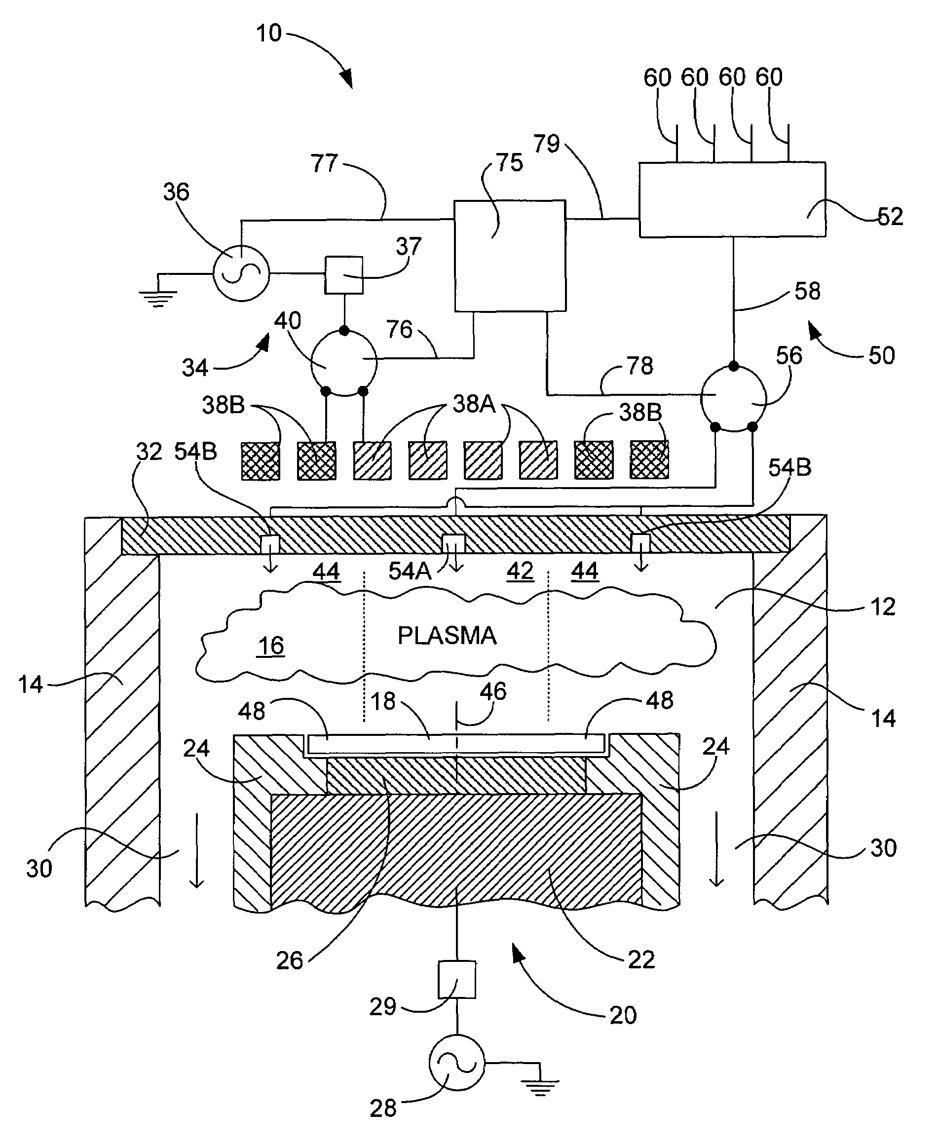
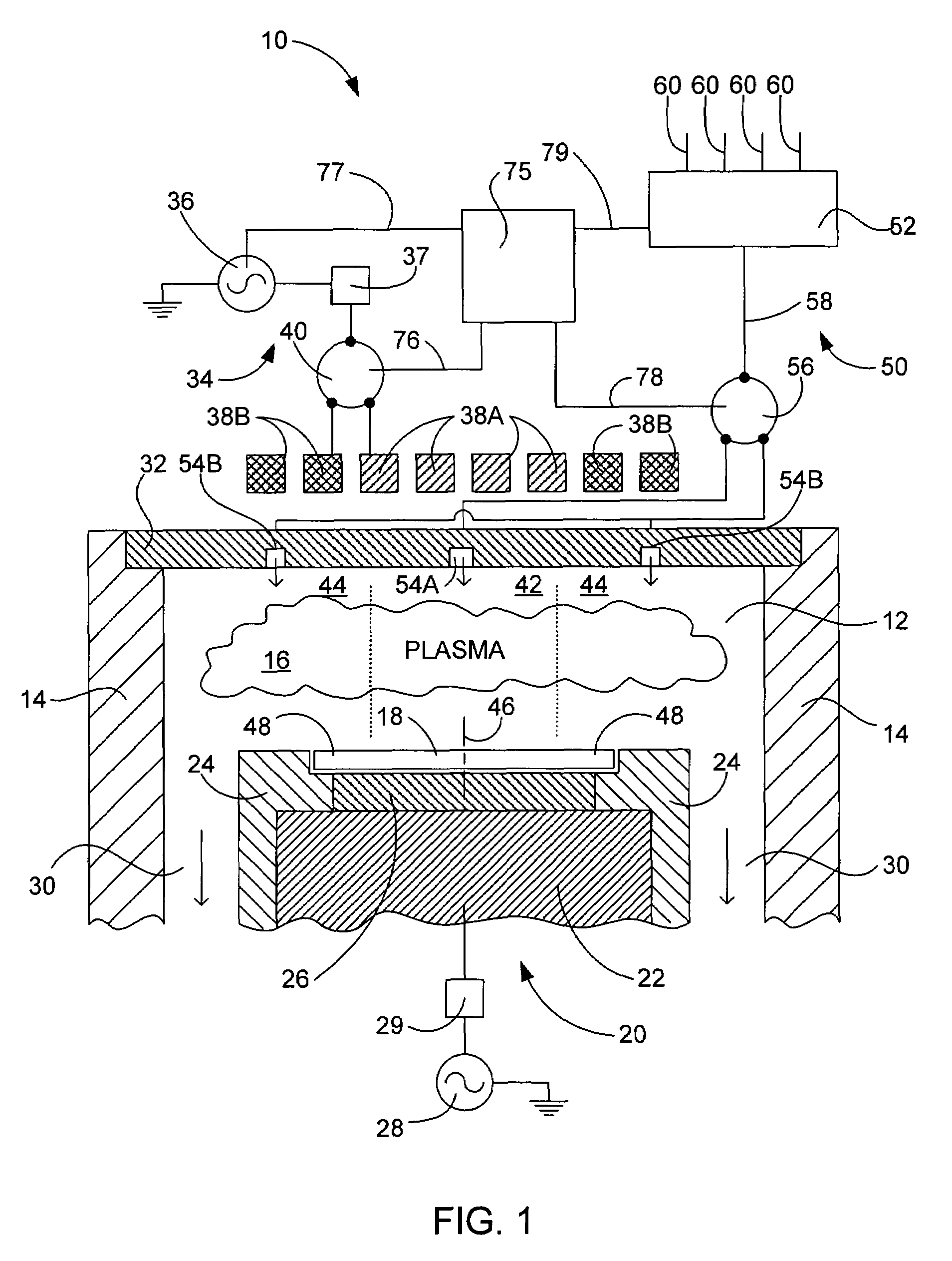
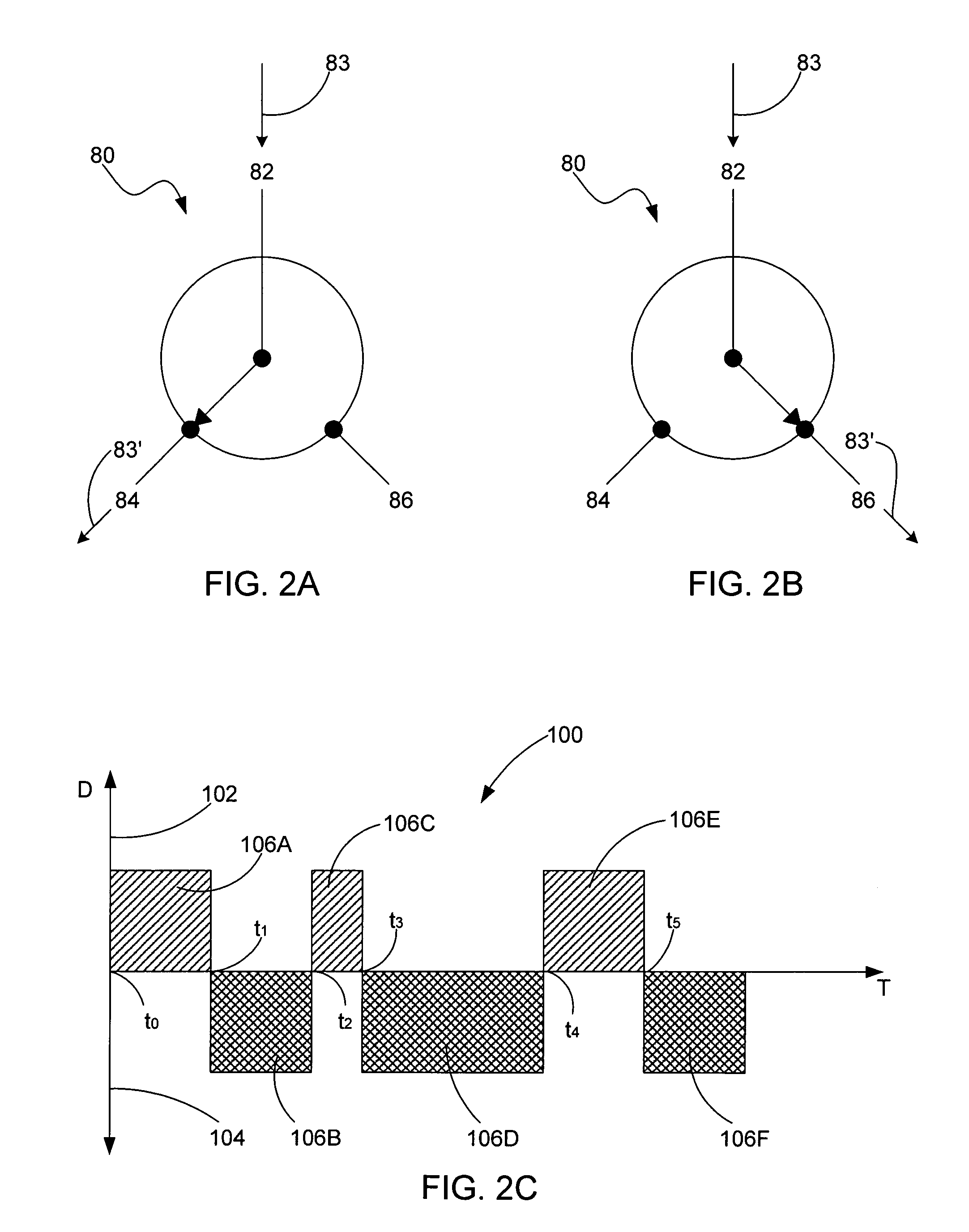
[0024]The invention pertains to an improved method and apparatus for uniformly processing a substrate. The present invention achieves process uniformity by enhancing the control over the distribution of components used to form reactants, which process a substrate inside a process chamber. These components are generally part of a process recipe and may include power, gas flow, temperature and the like. The invention is particularly useful in plasma processing systems where both ions and neutrals (e.g., reactants) are used to process a substrate. One aspect of the invention relates to spatially separating the distribution of a component into multiple and independent zones within a process chamber. Another aspect of the invention relates to switching (or spatially modulating) the distribution of the component, which is supplied from a single source, between each of the independent zones. Another aspect of the invention relates to varying the magnitude of the component and / or the compon...


PUM

PropertyMeasurementUnit
Timeaaaaaaaaaa
Flow rateaaaaaaaaaa
Concentrationaaaaaaaaaa

Abstract

A component delivery mechanism for distributing a component inside a process chamber is disclosed. The component is used to process a work piece within the process chamber. The component delivery mechanism includes a plurality of component outputs for outputting the component to a desired region of the process chamber. The component delivery mechanism further includes a spatial distribution switch coupled to the plurality of component outputs. The spatial distribution switch is arranged for directing the component to at least one of the plurality of component outputs. The component delivery mechanism also includes a single component source coupled to the spatial distribution switch. The single component source is arranged for supplying the component to the spatial distribution switch.

Description

CROSS REFERENCE TO RELATED APPLICATIONS[0001]The present application is a divisional application of U.S. application Ser. No. 09 / 607,599, filed Jun. 30, 2000, now U.S. Pat. No. 6,632,322 which is incorporated by reference herein in its entirety.BACKGROUND OF THE INVENTION[0002]The present invention relates to apparatus and methods for processing substrates such as semiconductor substrates for use in IC fabrication or glass panels for use in flat panel display applications. More particularly, the present invention relates to improved processing systems that are capable of processing substrates with a high degree of processing uniformity across the substrate surface.[0003]During the manufacture of a semiconductor-based product, for example, a flat panel display or an integrated circuit, multiple deposition and / or etching steps may be employed on the surface of a substrate to form devices such as transistors, capacitors, resistors, interconnects and the like. During deposition, success...

Claims


Application Information

Patent Timeline
IPC IPC(8): H05H1/24H01L21/302H05B6/00C23C16/00H05H1/46B01J4/00B01J19/08C23C16/50C23C16/52H01J37/32H01L21/205H01L21/3065
CPCH01J37/3244H01J37/321H01J37/32
Inventor GOTTSCHO, RICHARD A.STEGER, ROBERT J.
Owner LAM RES CORP
Why Eureka
Try Eureka