Method of making a solder ball
a solder ball and solder ball technology, applied in the field of solder ball, can solve the problems of serious problems, affecting the reliability of the bga, and creating voids in the solder layer
- Summary
- Abstract
- Description
- Claims
- Application Information
AI Technical Summary
Benefits of technology
Problems solved by technology
Method used
Image
Examples
embodiment 1
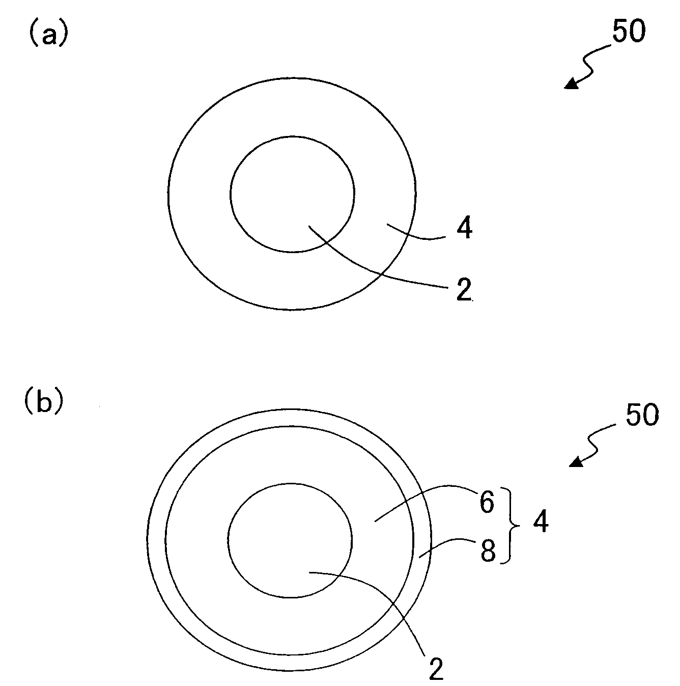
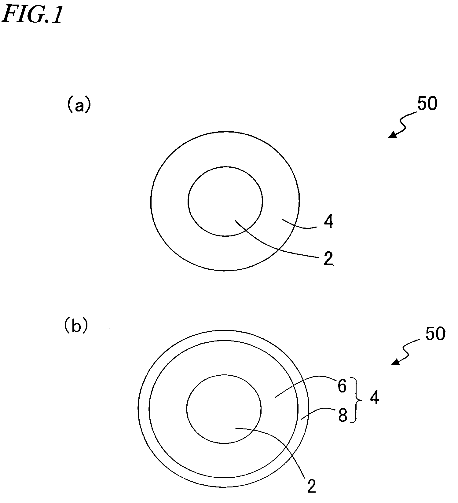
[0052]FIG. 1 is a cross-sectional view of a solder ball 50 according to a first preferred embodiment of the present invention. As shown in FIG. 1, the solder ball 50 includes a spherical core 2 and a solder layer 4, which includes Sn and Ag and which is provided so as to wrap up the core 2. The solder layer 4 may include either a single layer as shown in FIG. 1(a) or multiple layers as shown in FIG. 1(b). This solder layer 4 is controlled such that the amount of water contained in the solder layer 4 is 100 μl / g or less when represented by the amount of water vapor in standard conditions.
[0053]In this solder ball 50, the solder layer 4 is controlled so as to contain a sufficiently small amount of water as just described. Thus, the number of voids to be created while the solder layer 4 is being heated and melted can be reduced significantly. As will be described later for specific examples of the present invention, the present inventors confirmed via experiments that if the amount of ...
example 1
[0078]In a solder ball 50 representing a first specific example of the present invention, the solder layer 4 is a single Sn—Ag alloy layer. Hereinafter, a method of making the solder ball 50 of the first specific example will be described.
[0079]First, a spherical copper core with a diameter of 0.8 mm is pre-processed with a 17.5% HCl aqueous solution at room temperature for one minute (process step (a)). Next, the core is washed (immersed for one minute and rinsed for one minute) with pure water at room temperature (process step (b)). Subsequently, the core is immersed in an organic acid at room temperature for 30 seconds (process step (c)). Thereafter, the core is plated with a plating solution including tin methanesulfonate (24 g / l of Sn), silver methanesulfonate (1.4 g / l of Ag), sulfonic acid, hydroxycarboxylic acid, organophosphorus compound and thiourea (300° C.) at a current density of 0.30 A / dm2, thereby forming an Sn—Ag alloy plating layer (with a thickness of 35 μm) (step (...
example 2
[0081]In a solder ball 50 representing a second specific example of the present invention, the solder layer 4 consists of an Sn plating layer 6 and an Ag evaporation layer 8. Hereinafter, a method of making the solder ball 50 of the second specific example will be described.
[0082]First, a spherical copper core with a diameter of 0.5 mm is pre-processed with a 17.5% HCl aqueous solution at room temperature for one minute (process step (a)). Next, the core is washed (immersed for one minute and rinsed for one minute) with pure water at room temperature (process step (b)). Subsequently, the core is immersed in an organic acid at room temperature for 30 seconds (process step (c)). Thereafter, the core is plated with a plating solution including tin methanesulfonate (60 g / l of Sn) (40° C.) at a current density of 0.30 A / dm2, thereby forming an Sn plating layer (with a thickness of 34.2 μm) (step (d)). Then, the plating layer is washed (immersed for one minute and rinsed for one minute) w...
PUM
| Property | Measurement | Unit |
|---|---|---|
| thickness | aaaaa | aaaaa |
| mass % | aaaaa | aaaaa |
| thickness | aaaaa | aaaaa |
Abstract
Description
Claims
Application Information
 - R&D
- Intellectual Property
- Life Sciences
- Materials
- Tech Scout
- Unparalleled Data Quality
- Higher Quality Content
- 60% Fewer Hallucinations
Browse by: Latest US Patents, China's latest patents, Technical Efficacy Thesaurus, Application Domain, Technology Topic, Popular Technical Reports.
© 2025 PatSnap. All rights reserved.Legal|Privacy policy|Modern Slavery Act Transparency Statement|Sitemap|About US| Contact US: help@patsnap.com


