Mask, substrate with light reflective film, method for manufacturing light reflective film, liquid crystal display device, and electronic apparatus

a technology of light reflective film and substrate, which is applied in the direction of mirrors, instruments, photomechanical treatment, etc., can solve the problems of deterioration of display quality, large display quality degradation, and difficulty in making the surface facing the liquid crystal display device completely smooth, so as to reduce the occurrence of stains and effectively prevent interference fringes

Inactive Publication Date: 2007-08-14
BOE TECH GRP CO LTD
View PDF10 Cites 8 Cited by
  • Summary
  • Abstract
  • Description
  • Claims
  • Application Information

AI Technical Summary

Benefits of technology

[0016]That is, since the light transmissive or non-transmissive portions are randomly arranged, the substrate provided with the light reflective film exhibits excellent light scattering effect and effectively prevents the occurrence of the interference fringe.
[0051]Accordingly, such a light reflective film reflects light properly, and can reduce the occurrence of stains of various shapes and effectively prevent the occurrence of an interference fringe in the electronic apparatus.

Problems solved by technology

However, in such protective plate, it is difficult to make its surface facing the liquid crystal display device completely smooth, and fine concave portions or convex portions exist on the surface in many cases.
Therefore, in the case of providing such a protective plate on the liquid crystal display device, there is a problem that the display quality is greatly deteriorated due to the fine concave portions or convex portions on the surface.
One reason for the deterioration of the display quality is that the gap between the substrate at the viewing side and the protective plate in the liquid crystal display device is uneven due to the concavities or convexities existing on the surface of the protective plate.
That is, corresponding to the unevenness of the gap, interference occurs when light coming from the liquid crystal display device passes through the protective plate and as a result, interference fringes are generated.
It is presumed that the display quality is deteriorated because the generated interference fringes and the display images are mixed.
However, it is difficult to adjust the height precisely to effectively prevent the light interference because of the unevenness of the coating thickness, or the like.
In addition, since a reflective electrode is formed on the structure having the plurality of concaves or convexes of different heights, there often occurs a breaking of wire or short circuit, too.
In addition, the disclosed method for manufacturing a light reflective film involves many processing steps and management items to be processed, which results in many problems in the manufacture.
Therefore, according to the light reflective film disclosed in Japanese Unexamined Patent Application Publication No. 6-27481, it is not only difficult to prevent the occurrence of interference fringes effectively, but also difficult to manufacture such light reflective film stably and effectively.
Although the above-proposed methods reduce the occurrence of the interference fringe, a new problem has been found that stains of various shapes are seen on a screen, thereby causing remarkable deterioration of display quality.

Method used


Image

  • Mask, substrate with light reflective film, method for manufacturing light reflective film, liquid crystal display device, and electronic apparatus
  • Mask, substrate with light reflective film, method for manufacturing light reflective film, liquid crystal display device, and electronic apparatus
  • Mask, substrate with light reflective film, method for manufacturing light reflective film, liquid crystal display device, and electronic apparatus

Examples


first embodiment

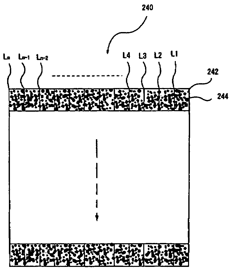
[0081]In a first embodiment of the present invention, as shown in FIG. 1, there is provided a mask 10 to manufacture a substrate with a light reflective film. The mask 10 includes light transmissive or non-transmissive portions randomly arranged in the plane direction in 100 to 2,000 RGB dot units or the whole screen unit. As shown in FIG. 1, a stripe-shaped random pattern in a plurality of rows W1 to W18 and in a plurality of columns L1 to L54 is formed and repeated in a plurality of lines to obtain the light transmissive or non-transmissive portions.

[0082]The random arrangement of the light transmissive or non-transmissive portions simply means a disorderly arrangement of the light transmissive or non-transmissive portions. More exactly, it means that in case that the mask is cut into a plurality of unit areas and the cut unit areas of the mask are stacked, patterns of the cut unit areas are completely different, or partially similar but not completely.

[0083]1. Light Transmissive ...

second embodiment

[0130]In a second embodiment of the present invention, as shown in FIG. 6, there is provided a substrate 70 provided with a light reflective film including a base 77 and a reflective layer 72. A plurality of convex portions 76 formed on the surface of the base 77 are randomly arranged in the plane direction in 100 to 2,000 RGB dot units or a whole screen unit. Herein, for example, a negative type photosensitive resin is used.

[0131]1. Base

[0132]As shown in FIG. 6, preferably, the base 77 includes a first base 76 and a second base 79 formed over the first base 76. The first base 76 includes a plurality of separated (independent) or partially overlapped convex portions, and the second base 79 is a continuous layer.

[0133]Thereby, it is possible to form a reflective layer 72 with a comparatively gently curved surface by disposing the continuous second base 79 on the first base 76. Accordingly, when the substrate 70 provided with the reflective layer 72 is used in liquid crystal display d...

third embodiment

[0187]In a third embodiment, there is provided a method for manufacturing a light reflective film including a base and a reflective layer. The method comprises the steps of: (a) forming a first base including a plurality of concave portions or convex portions by performing an exposure process on an applied photosensitive resin using a mask in which light transmissive or non-transmissive portions are randomly arranged in the plane direction in 100 to 2,000 RGB dot units or a whole screen unit; (b) forming a second base including a plurality of continuous concave portions or convex portions by applying a photosensitive resin on the surface of the first base and subsequently performing an exposure process on the applied photosensitive resin; and (c) forming a reflective layer on the surface of the second base.

[0188]Hereinafter, with reference to FIGS. 10 and 11, the method for manufacturing the light reflective film (the substrate with the light reflective film), in which convex portio...


PUM

PropertyMeasurementUnit
diameteraaaaaaaaaa
diametersaaaaaaaaaa
area ratioaaaaaaaaaa

Abstract

A substrate is provided with a light reflective film including a base and a reflective layer, in which a plurality of concave portions or convex portions formed on the surface of the base are randomly arranged in the plane direction in 100 to 2,000 RGB dot units or a whole screen unit, are formed using a mask in which light transmissive or non-transmissive portions are randomly arranged in the plane direction in 100 to 2,000 RGB dot units or the whole screen unit.

Description

CROSS REFERENCE TO RELATED APPLICATIONS[0001]This application is a divisional patent application of U.S. Ser. No. 10 / 410,518 filed Apr. 9, 2003 now U.S. Pat. No. 7,060,396, claiming priority to Japanese Application No. 2002-108529 filed Apr. 10, 2002, all of which are hereby incorporated by reference.BACKGROUND[0002]1. Technical Field of the Invention[0003]The present invention relates to a mask, a substrate with a light reflective film, a method for manufacturing a light reflective film, an optical display device, and an electronic apparatus, and more specifically, it relates to a mask for manufacturing a substrate with a light reflective film generating few interference fringes, a substrate with a light reflective film formed by using the mask, a method for manufacturing a light reflective film, an optical display device having a light reflective film on which hardly any interference fringes are generated, and an electronic apparatus having a light reflective film on which hardly ...

Claims


Application Information

Patent Timeline
Patent Type & Authority Patents(United States)
IPC IPC(8): G02F1/1335G02B5/02G02B5/08G02B5/28G02B27/00G03F1/52G03F1/70
CPCG02B5/0242G02B5/0278G03F1/14G02B27/0025G02F1/133555G02B5/08G03F1/00G02F1/1333
Inventor OTAKE, TOSHIHIROMATSUO, MUTSUMITSUYUKI, TADASHI
Owner BOE TECH GRP CO LTD
Why Eureka
Try Eureka