Electrical connector having an oscillating multilayered conducting body

a multi-layered, conducting body technology, applied in the direction of coupling contact members, coupling device details, coupling device connections, etc., can solve the problems of complex shape, deformation of conducting pins, and difficult manufacturing processes, and achieve the effect of reducing for

Active Publication Date: 2007-08-14
LOTES
View PDF12 Cites 17 Cited by
  • Summary
  • Abstract
  • Description
  • Claims
  • Application Information

AI Technical Summary

Benefits of technology

[0013]Because the line connected between the two contacting points and the upper surface of the insulating body has an angle, the contacting points are not located at a vertical straight line. When the conducting body is compressed, the conducting body can deform and oscillates to reduce the force imposed on the contacting points. The goals of the first embodiment are achieved and the chaps produced on the metal layer are avoided.

Problems solved by technology

However, because these conducting pins are manufactured from a general metal material, the shape is complex and the manufacturing process difficult.
After the conducting pin is compressed or bent a number of times, the conducting pin becomes deformed and its flexibility worsens.
Therefore, the contact between the electrical connector and the electronic element becomes worse in that the function of the electrical connector is affected.

Method used


Image

  • Electrical connector having an oscillating multilayered conducting body
  • Electrical connector having an oscillating multilayered conducting body
  • Electrical connector having an oscillating multilayered conducting body

Examples


Embodiment Construction

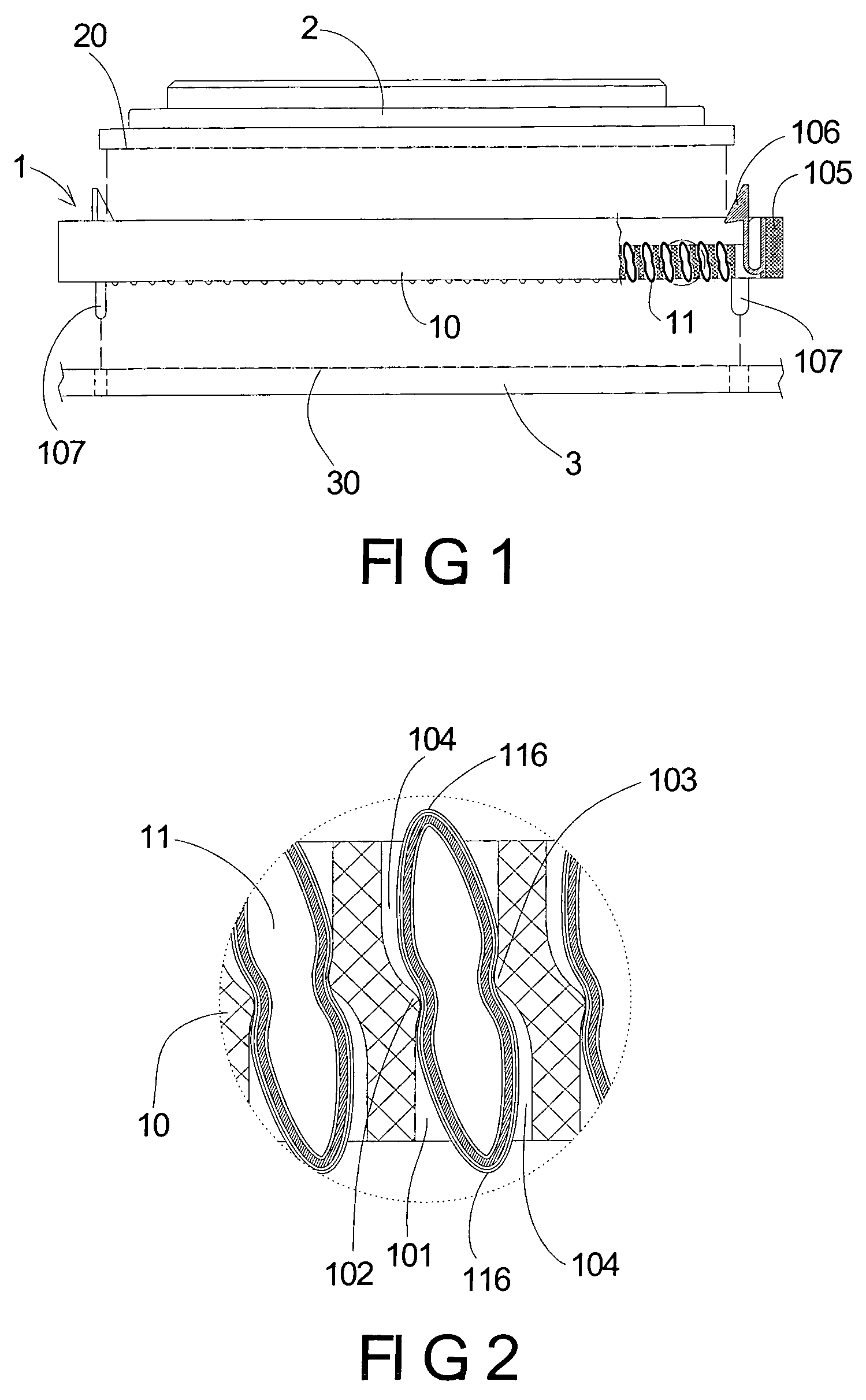
[0021]Reference is made to FIGS. 1˜3. The electrical connector 1 of the present invention is used for connecting the chip module 2 to the circuit board 3. The electrical connector 1 includes an insulating body 10 and conducting bodies 11.

[0022]The insulating body 10 has a plurality of receiving holes 101 that pass through the upper surface and the lower surface of the insulating body 10. The conducting bodies 11 are received in the receiving holes 101. On the inner wall of the receiving hole 101, there is a positioning mechanism for positioning the conducting body 11. In this embodiment, the positioning mechanism is comprised of two protruding parts 102, 103 that are located at two sides of the inner wall of the receiving hole 101 and are staggered to each other in a vertical direction. When the conducting body 11 is compressed, the conducting body 11 can oscillate in the receiving hole 101. At the upper and lower corresponding locations of the inner wall of the receiving hole 101 i...


PUM


Abstract

An electrical connector is used for connecting a chip module to a circuit board. The electrical connector includes an insulating body having a plurality of receiving holes, and conducting bodies located in the receiving holes. The conducting body includes a flexible body and a metal layer located on the outside of the flexible body. Because the conducting body of the electrical connector includes a flexible body and a metal layer located on the outside of the flexible body, the flexibility of the conducting body is assured. The external metal layer can make the chip module electrically connect firmly with the circuit board. Therefore, the connection between the chip module and the circuit board is assured.

Description

BACKGROUND OF THE INVENTION[0001]1. Field of the Invention[0002]The present invention relates to an electrical connector. In particular, this invention relates to a compressing contact electrical connector.[0003]2. Description of the Related Art[0004]The compressing contact electrical connector of the prior art generally includes an insulating body, and conducting pins received in the insulating body. The insulating body has pin-receiving grooves and the conducting pins are received in the pin-receiving grooves. The conducting pin includes a fastening part and two contacting parts located at two ends of the conducting pins. Two butting electronic elements are compressed so as to contact each other so that the two butting electronic elements are electrically connected together, such as in China patent, CN 00217081.7. However, because these conducting pins are manufactured from a general metal material, the shape is complex and the manufacturing process difficult. After the conducting...

Claims


Application Information

Patent Timeline
Patent Type & Authority Patents(United States)
IPC IPC(8): H01R12/00H05K1/00
CPCH01R13/03H01R13/2414H01R12/714
Inventor JU, TED
Owner LOTES
Why Eureka
Try Eureka