Laser-based cleaning device for film analysis tool

a technology of film analysis and cleaning device, which is applied in the direction of material analysis using wave/particle radiation, optical radiation measurement, semiconductor/solid-state device testing/measurement, etc., can solve the problem of small damage risk to test sample, and achieve accurate and repeatable analysis of thin film, reduce the total footprint, and eliminate any delays

Active Publication Date: 2007-08-07
KLA CORP
View PDF26 Cites 27 Cited by
  • Summary
  • Abstract
  • Description
  • Claims
  • Application Information

AI Technical Summary

Benefits of technology

[0011]The present invention provides localized contaminant layer removal from a thin film surface, thereby enabling accurate and repeatable analysis of the thin film by a measurement tool. By using a concentrated energy beam to clean only the portion of the thin film to be measured by the measurement tool, the thin film analysis can be performed without the long heating and cooling times associated with conventional cleaning systems. Furthermore, the compact components used in an energy beam-based cleaning system can be incorporated into the thin film measurement tool itself, thereby eliminating any delays related to transferring the wafer to and from a stand-alone cleaning system. This integration also minimizes the total footprint required for a thin film analysis system, and since the wafer can be cleaned and analyzed in the same process chamber, redeposition of contaminants on the cleaned portion of the wafer can be prevented.
[0012]A thin film analysis system in accordance with an embodiment of the present invention comprises an energy beam source, an analysis module, and a stage. The stage holds a test sample (such as a wafer) that includes a thin film layer to be measured by the analysis module. The analysis module can comprise any thin film analysis system or systems, including a single-wavelength ellipsometer (SWE, such as described in co-owned, co-pending U.S. patent application Ser. No. 09 / 298,007), a spectroscopic ellipsometer (SE, such as described in co-owned U.S. Pat. No. 5,608,526), a reflectometer (such as described in co-owned U.S. Pat. No. 5,747,813), a non-contact electrical measurement system (such as described in co-owned U.S. Pat. No. 5,485,091), a GXR system (such as described in co-owned, co-pending U.S. patent application [Attorney Docket KLA-001]), a contact-based electrical measurement system, an XRF system, and / or an EMP system. More generally, this cleaning system can be used with any sort of inspection or metrology system used in the production of semiconductor devices. According to an embodiment of the present invention, the energy beam source is incorporated into a conventional thin film analysis tool, thereby minimizing the total footprint of the thin film analysis system.
[0013]The energy beam source is configured to direct an energy beam at a contaminant layer on the surface of the thin film layer. The energy beam heats a portion of the contaminant layer until that portion of the contaminant layer is vaporized. This process can be aided by direct photon excitation of the bonds between the contaminant layer and the thin film layer. The area of the thin film layer exposed by this cleaning operation can then be analyzed by the analysis module. The size of this analysis area required by the analysis module for performance of the thin film analysis can be used to determine the minimum required power and size of the energy beam. By minimizing the power and size of the energy beam, the risk of damage to the test sample is small. This risk of damage can be further reduced by performing the cleaning and measuring operations at non-functional regions of the test sample. According to an embodiment of the present invention, the energy beam source can comprise a laser, such as a Q-switched pulsed laser. According to another embodiment of the present invention, the energy beam source can comprise a flashlamp with appropriate focusing optics.
[0014]According to an embodiment of the present invention, a probe beam generated by the analysis module (e.g., a low-power laser beam, a white light beam, a corona discharge, an x-ray beam, etc.) is directed at the same location on the test sample as the energy beam produced by the energy beam source. Alternatively, a physical probe structure (e.g., a four-point probe in a spreading resistance tool) (can be aimed at the same location on the test sample as the energy beam produced by the energy beam source. Consequently, the test sample does not need to be moved between the cleaning and measurement operations, thereby maximizing analysis throughput. Furthermore, because the measurement operation can be performed immediately after the cleaning operation, the chances of the cleaned portion of the thin film layer (i.e., the analysis area) being recontaminated before the measurement operation are minimized.
[0015]According to another embodiment of the present invention, the probe beam (or probe structure) from the analysis module and the energy beam are directed at different locations on the test sample. The test sample (and / or the analysis module) is then repositioned after the cleaning operation to align the probe beam (or probe structure) with the analysis area of the thin film layer. This allows the focusing optics or probe structure of the analysis module to be kept out of the vicinity of the portion of the contaminant layer being vaporized, thereby minimizing the risk of any contaminant redeposition on the measurement focusing optics or probe structure.

Problems solved by technology

By minimizing the power and size of the energy beam, the risk of damage to the test sample is small.

Method used


Image

  • Laser-based cleaning device for film analysis tool
  • Laser-based cleaning device for film analysis tool
  • Laser-based cleaning device for film analysis tool

Examples


Embodiment Construction

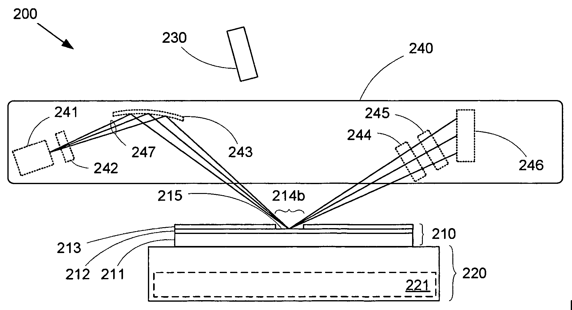
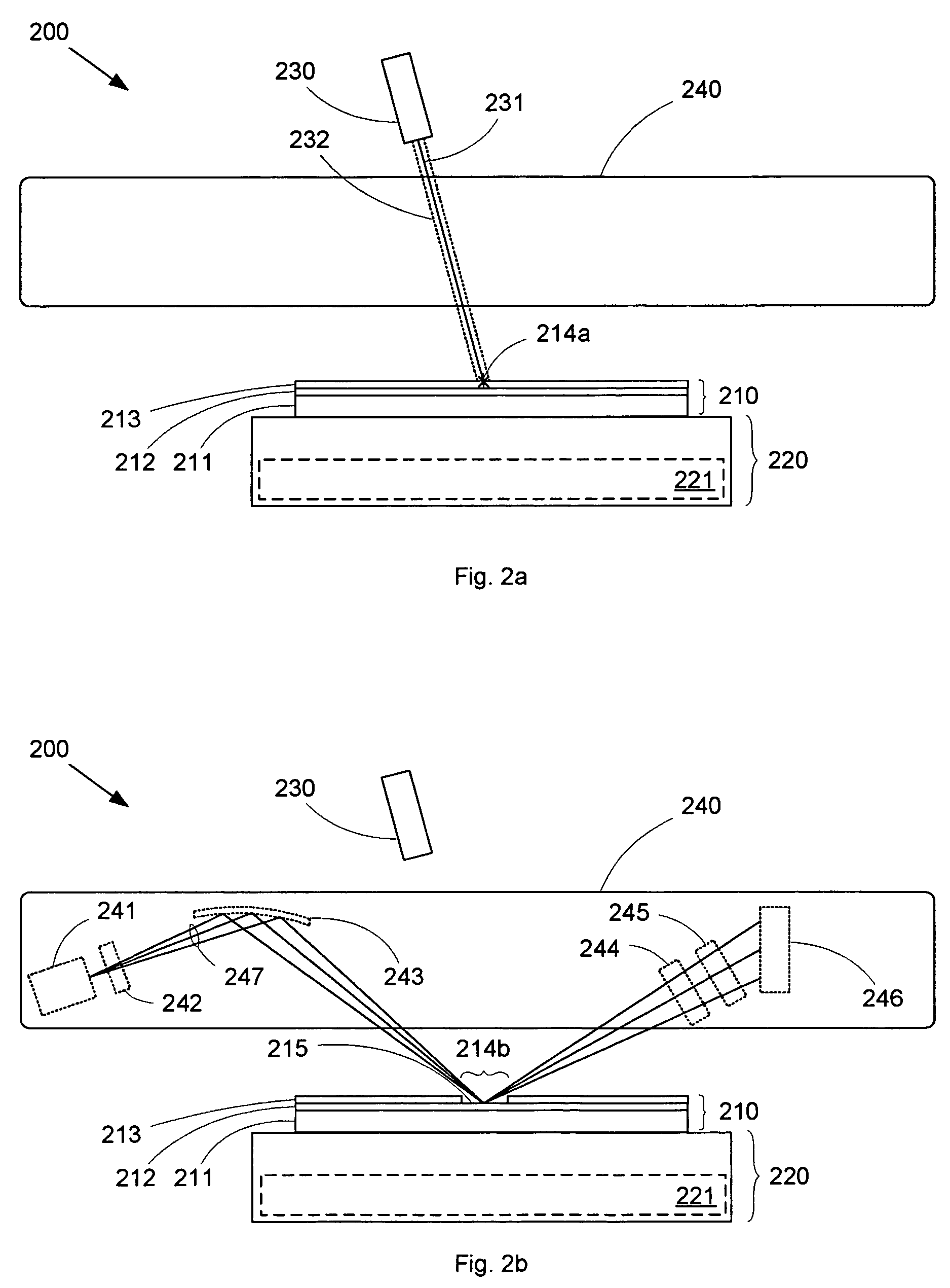
[0020]FIG. 2a shows a thin film analysis system 200 in accordance with an embodiment of the present invention. Analysis system 200 comprises a stage 220, an energy beam source 230, and an analysis module 240. Stage 220 holds a test sample 210 that comprises a thin film layer 212 formed on a substrate 211. Substrate 211 can comprise any structure on which thin film layer 212 can be formed, including a single-layer structure (such as a silicon wafer) or a multi-layer structure (such as an additional thin film layer or layers formed on a silicon wafer). Test sample 210 also includes a contaminant layer 213 formed on the surface of thin film layer 212. Contaminant layer 213 can comprise any unwanted material on the surface of thin film layer 212.

[0021]An analysis operation performed using analysis system 200 actually comprises two steps—a cleaning operation and a measurement operation. During the cleaning operation, a small portion of contaminant layer 213 is removed. The exposed portio...


PUM

PropertyMeasurementUnit
widthaaaaaaaaaa
wavelengthaaaaaaaaaa

Abstract

A system for analyzing a thin film uses an energy beam, such as a laser beam, to remove a portion of a contaminant layer formed on the thin film surface. This cleaning operation removes only enough of the contaminant layer to allow analysis of the underlying thin film, thereby enhancing analysis throughput while minimizing the chances of recontamination and / or damage to the thin film. An energy beam source can be readily incorporated into a conventional thin film analysis tool, thereby minimizing total analysis system footprint. Throughput can be maximized by focusing the probe beam (or probe structure) for the analysis operation at the same location as the energy beam so that repositioning is not required after the cleaning operation. Alternatively, the probe beam (structure) and the energy beam can be directed at different locations to reduce the chances of contamination of the analysis optics.

Description

BACKGROUND OF THE INVENTION[0001]1. Field of the Invention[0002]The present invention relates to field of thin film measurement, and in particular to a method and apparatus for cleaning the surface of a thin film to improve measurement accuracy.[0003]2. Background of the Invention[0004]As the dimensions of semiconductor devices continue to shrink, accurate and efficient characterization of the components forming those devices becomes more critical. Typically, the manufacturing process for modern semiconductor devices includes the formation of a number of layers or “thin films” on a silicon wafer. The thin films can include oxide, nitride, and / or metal layers, among others. To ensure proper performance of the finished semiconductor devices, the thickness and composition of each thin film formed during the manufacturing process must be tightly controlled.[0005]Modern thin films have reached the point where the accuracy and reproducibility of thin film measurements can be limited by co...

Claims


Application Information

Patent Timeline
Patent Type & Authority Patents(United States)
IPC IPC(8): G01J4/00B08B3/12B08B6/00B08B7/00B08B7/02C25F1/00C25F3/30C25F5/00G01B11/24G01B11/28G01B11/30G01B15/02G01N21/55G01N21/86G01N23/00G01N23/223G01R27/26G01R31/26G01R31/302G01R31/305G01T1/36G01V8/00G02F1/01G21K7/00H01J40/14H01L21/66G01N21/21
CPCG01N21/211
Inventor JANIK, GARY R.MAXTON, PATRICK M.
Owner KLA CORP
Why Eureka
Try Eureka