Charge-device model electrostatic discharge protection using active device for CMOS circuits

a technology of electrostatic discharge protection and charge device, which is applied in the direction of semiconductor devices, semiconductor/solid-state device details, electrical apparatus, etc., can solve the problems of damage or destruction of ic, and conventional esd protection schemes, such as those described above, may no longer be effective in protecting gate oxides

Inactive Publication Date: 2007-08-07
IND TECH RES INST
View PDF13 Cites 11 Cited by
  • Summary
  • Abstract
  • Description
  • Claims
  • Application Information

AI Technical Summary

Benefits of technology

[0019]Still in accordance with the present invention, there is provided a method for providing electrostatic discharge protection that includes providing a contact pad, grounding the contact pad, providing a transistor having a substrate, providing an active device CDM clamp coupled between the contact pad and the substrate of the transistor, accumulating electrostatic charges in the substrate of the transistor, and conducting the accumulated electrostatic charges in the substrate of the transistor to the contact pad.

Problems solved by technology

A semiconductor integrated circuit (“IC”) is generally susceptible to an electrostatic discharge (“ESD”) event, which may damage or destroy the IC.
With the advance of semiconductor technology into a deep sub-micron era, the conventional ESD protection schemes, such as those described above, may no longer be effective in protecting gate oxides that are as thin as 4 na iiefes nanometers (tim) or less from a CDM ESD event.

Method used


Image

  • Charge-device model electrostatic discharge protection using active device for CMOS circuits
  • Charge-device model electrostatic discharge protection using active device for CMOS circuits
  • Charge-device model electrostatic discharge protection using active device for CMOS circuits

Examples


Embodiment Construction

[0042]Reference will now be made in detail to the present embodiments of the invention, examples of which are illustrated in the accompanying drawings. Wherever possible, the same reference numbers will be used throughout the drawings to refer to the same or like parts.

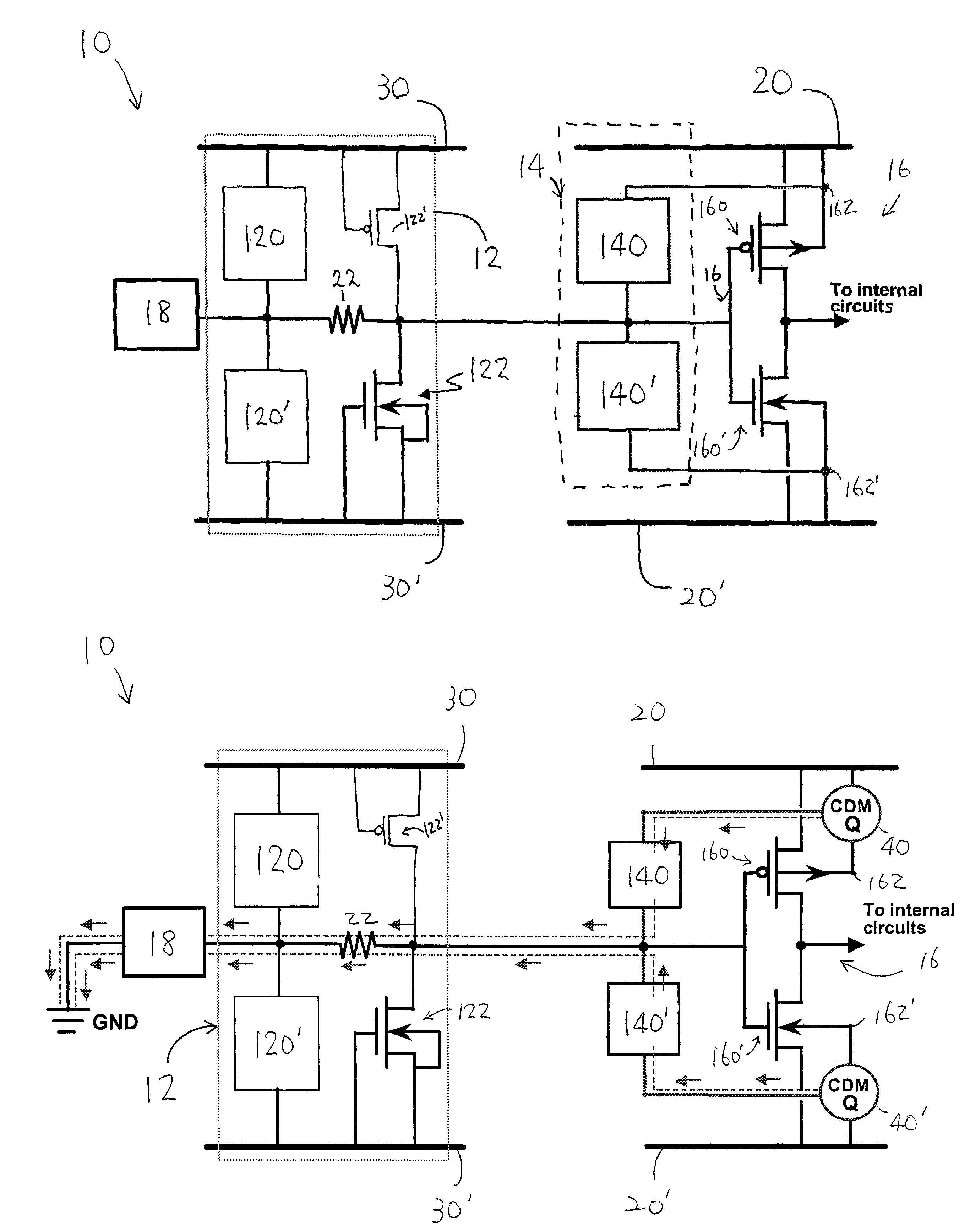
[0043]FIG. 6A shows a circuit 10 for ESD protection in accordance with one embodiment of the present invention. Referring to FIG. 6A, the circuit 10 includes an HBM / MM ESD protection circuit 12 and a CDM ESD protection circuit 14. CDM ESD protection circuit 14 includes a first CDM clamp 140 for protecting a CMOS device 16 from a CDM ESD event. CDM clamp 140 is coupled to a contact pad 18 through a resistor 22 provided in ESD protection circuit 12 and a substrate 162 of a PMOS transistor 160 of CMOS device 16 such that electrostatic charges accumulated in substrate 162 of PMOS transistor 160 may be quickly conducted by CDM clamp 140 to contact pad 18 during a CDM ESD event. In one embodiment, contact pad 18 is an input...


PUM


Abstract

An integrated circuit for providing electrostatic discharge protection that includes a contact pad, a CMOS device including a transistor having a substrate, and a CDM clamp for providing electrostatic discharge protection coupled between the contact pad and the CMOS device, the CDM clamp including at least one active device, wherein the CDM clamp conducts electrostatic charges accumulated in the substrate of the transistor to the contact pad and wherein the CMOS device is coupled between a high voltage line and a low voltage line.

Description

RELATED APPLICATION[0001]This application is related to U.S. patent application Ser. No. 10 / 230,055, entitled “ELECTROSTATIC DISCHARGE PROTECTION DEVICE AND METHOD OF MANUFACTURING THE SAME,” filed on Aug. 29, 2002, U.S. patent application Ser. No. 10 / 230,287, entitled “ELECTROSTATIC DISCHARGE PROTECTION CIRCUIT WITH AN ACTIVE DEVICE,” filed on Aug. 29, 2002, and U.S. patent application Ser. No. 09 / 749,377, entitled “SUBSTRATE-BIASED SILICON DIODE FOR ELECTROSTATIC DISCHARGE PROTECTION AND FABRICATION METHOD,” filed on Dec. 28, 2000. The related applications are expressly incorporated herein by reference.FIELD OF THE INVENTION[0002]This invention pertains in general to circuits and methods for electrostatic discharge (“ESD”) protection and, more particularly, to circuits and methods for a charged-device model (“CDM”) ESD protection using active ESD devices.BACKGROUND OF THE INVENTION[0003]A semiconductor integrated circuit (“IC”) is generally susceptible to an electrostatic discharg...

Claims


Application Information

Patent Timeline
Patent Type & Authority Patents(United States)
IPC IPC(8): H01L21/336H01L23/60H01L27/02
CPCH01L27/0266
Inventor KER, MING-DOUTSENG, TANG-KUIJIANG, HSIN-CHIN
Owner IND TECH RES INST
Why Eureka
Try Eureka