Liquid crystal display and electronic device

a technology of liquid crystal display and electronic device, which is applied in the direction of liquid crystal compositions, instruments, chemistry apparatus and processes, etc., can solve the problems of reducing contrast, non-uniformity will be visible, and alignment disorder of liquid crystals, so as to improve the quality of reflective display and transmissive display, the effect of high voltage and intense electric field

Inactive Publication Date: 2007-07-31
SEIKO EPSON CORP
View PDF22 Cites 3 Cited by
  • Summary
  • Abstract
  • Description
  • Claims
  • Application Information

AI Technical Summary

Benefits of technology

[0017]The liquid crystal display according to the invention preferably further can include a circularly polarized light inputting device that inputs circularly polarized light to the element substrate and the opposite substrate. By this structure, the quality of reflective display and transmissive display is further improved. If circularly polarized light is used, it is not necessary to determine the direction in which the liquid crystal molecules tilt when the voltage is applied. Regardless of the direction, if the liquid crystal molecules tilt by the voltage, a bright display is achieved.
[0018]In the liquid crystal display according to the present invention, the switching element may be a nonlinear diode element. A TFD (thin film diode) element needs comparatively high voltage for switchi

Problems solved by technology

In addition, since alignment areas of the liquid crystal have different vision properties, non-uniformity will disadvantageously

Method used


Image

  • Liquid crystal display and electronic device
  • Liquid crystal display and electronic device
  • Liquid crystal display and electronic device

Examples


Embodiment Construction

[0027]Embodiments of the invention will now be described with reference to the drawings.

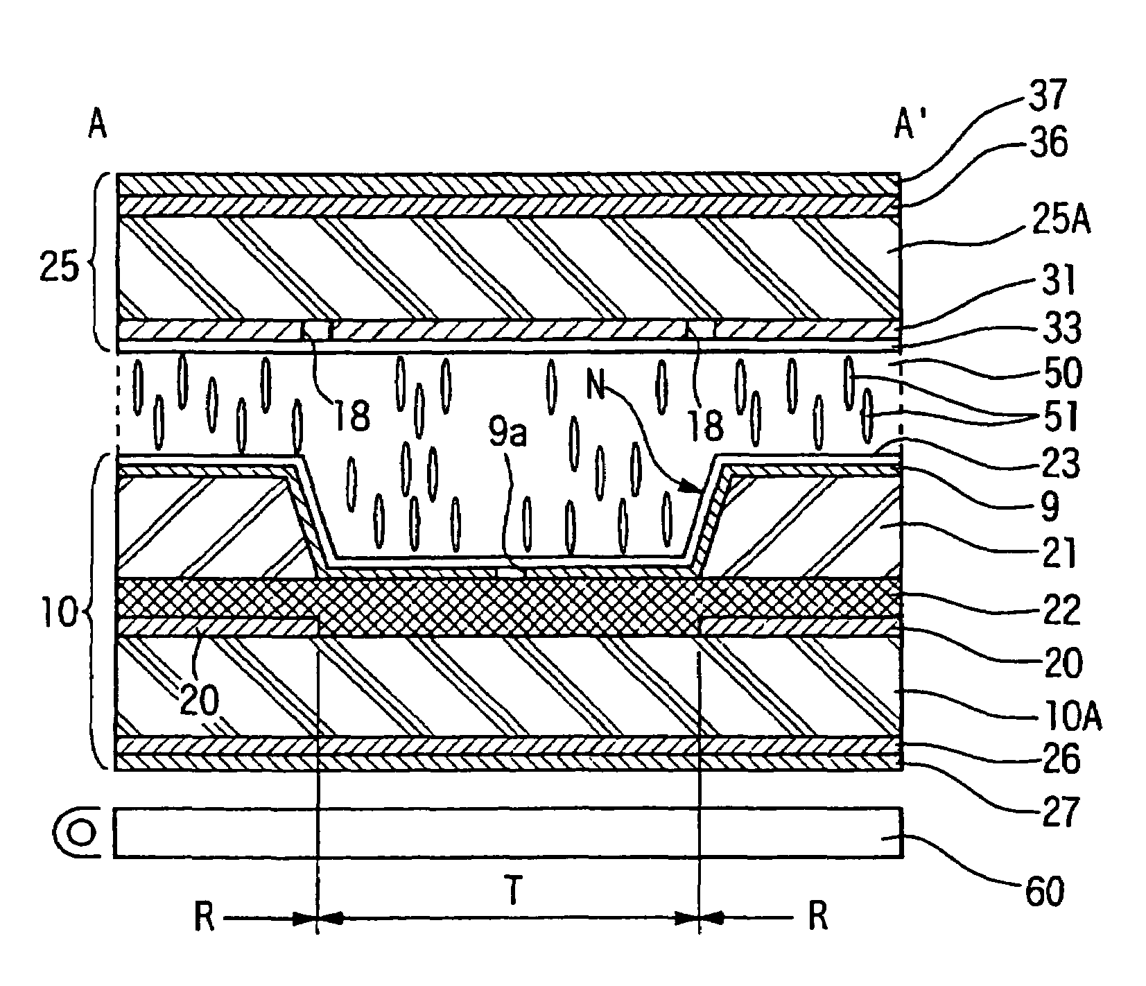
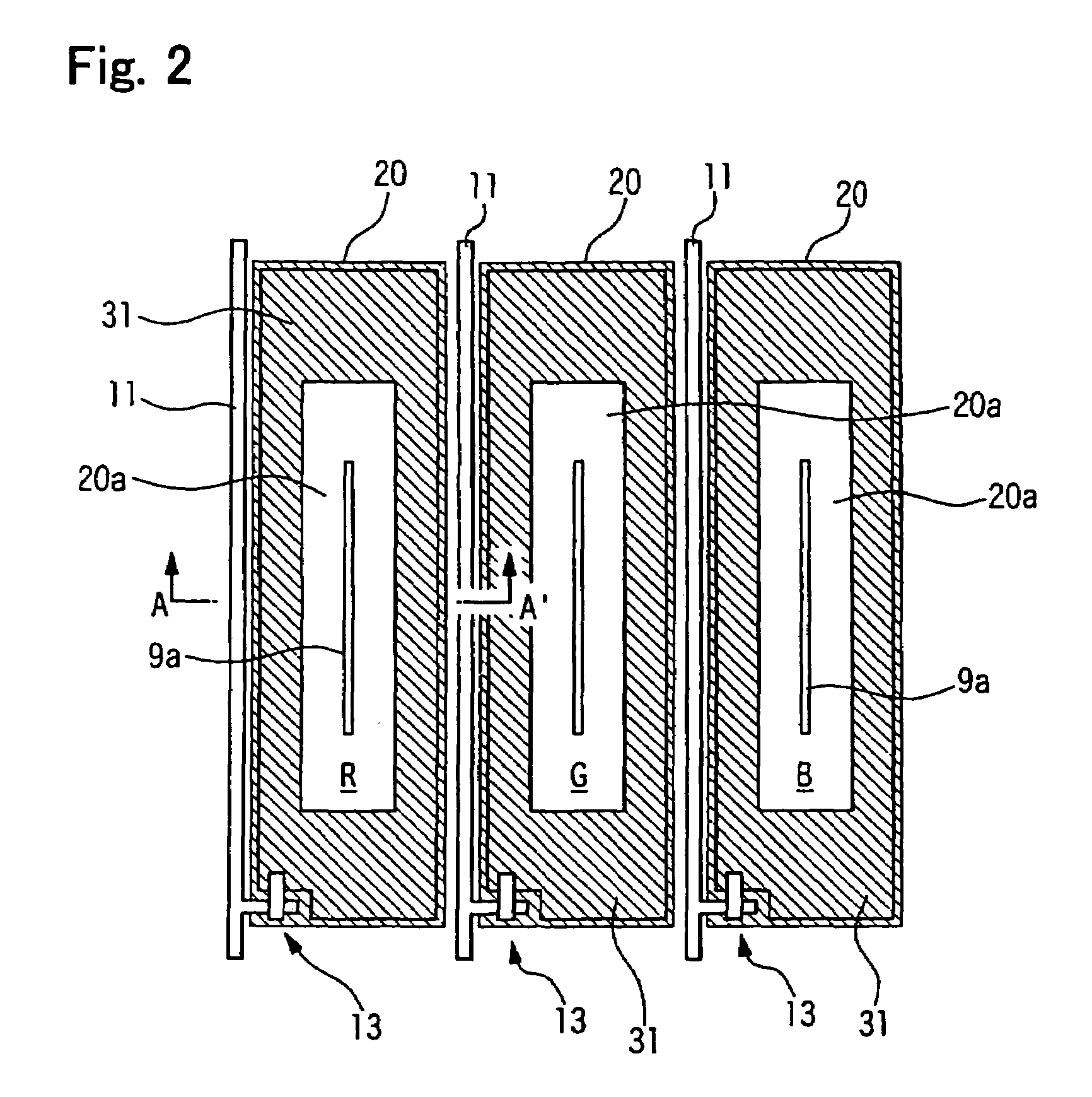
[0028]FIG. 1 is a perspective view showing a display area of a liquid crystal display of the first embodiment of the invention. FIG. 2 is a plan view showing the structure of one pixel area. FIG. 3 is a sectional view taken along line A-A′ of FIG. 2. The liquid crystal display shown in these figures is an active-matrix color liquid crystal display including TFD (thin film diode) elements (nonlinear diode elements) functioning as switching elements. As shown schematically in FIG. 3, the liquid crystal layer of this embodiment is formed of liquid crystal with negative dielectric anisotropy and the initial alignment state of molecules of the liquid crystal is vertical.

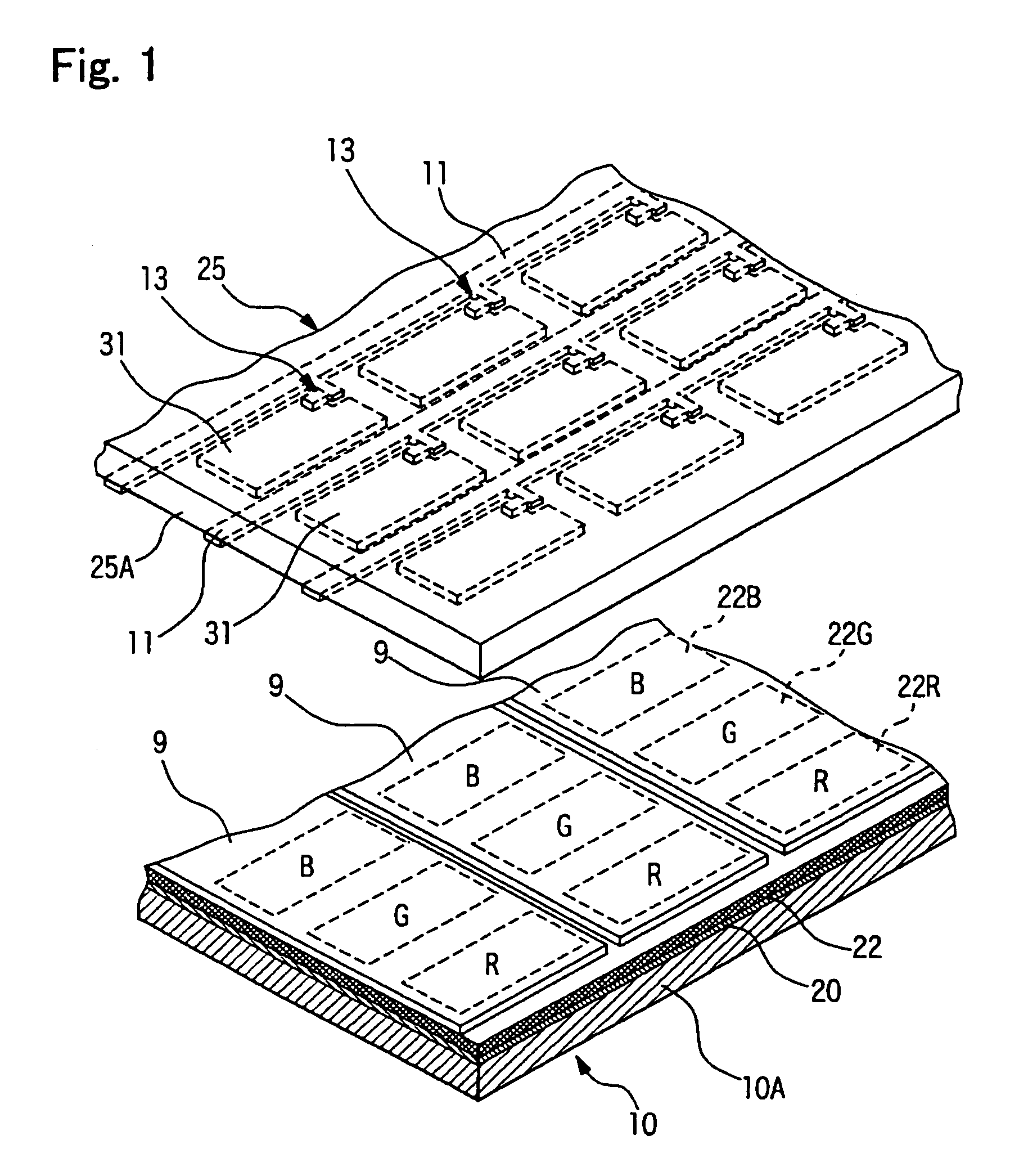
[0029]As shown in FIG. 1, the liquid crystal display of this embodiment is composed mainly of an element substrate 25 and an opposite substrate 10 facing each other. A liquid crystal layer (not shown) is disposed between the substrates...


PUM


Abstract

The invention provides a liquid crystal display having uniform display and having a wide viewing angle despite the fact that the display includes active elements for switching pixels in the display area, and an electronic device including the same. Specifically, the invention is a transflective liquid crystal display, each dot of which has a reflective display area and a transmissive display area. The liquid crystal display can include an element substrate having a plurality of pixel electrodes, each pixel electrode being provided with a thin film diode (TFD) element, and an opposite substrate facing the element substrate. A reflective layer formed on the opposite substrate extends directly below the TFD element.

Description

BACKGROUND OF THE INVENTION[0001]1. Field of Invention[0002]The present invention relates to a liquid crystal display and an electronic device.[0003]2. Description of Related Art[0004]Transflective liquid crystal displays can include a liquid crystal layer disposed between an upper substrate and a lower substrate. The inner surface of the lower substrate is provided with a reflective film formed of metal, such as aluminum. The reflective film has an opening for transmitting light and functions as a transflector. In order to improve brightness and contrast, a transflective liquid crystal display having a structure called multi-gap structure is disclosed. See, for example, Japanese Unexamined Patent Application Publication No. 11-242226. In this structure, the thickness of the liquid crystal layer is different between the reflective display area and the transmissive display area. The reflective display area corresponds to the area in which the reflective film is formed. The transmissi...

Claims


Application Information

Patent Timeline
IPC IPC(8): G02F1/1335G02F1/1333G02F1/1343G02F1/1365
CPCG02F1/134309G02F1/133371G02F2203/09G02F2001/133541G02F1/133541G02F1/1335
Inventor MAEDA, TSUYOSHI
Owner SEIKO EPSON CORP
Why Eureka
Try Eureka