
Apparatus for statistical LSI delay simulation

a delay simulation and statistical technology, applied in the field of statistical delay simulation apparatus, can solve the problems of increased useless parts in the design, increased performance (e.g., operation frequency), and increased possibility of malfunction, and improve the possibility of lack of quality

Inactive Publication Date: 2007-07-03
PANASONIC CORP
View PDF18 Cites 42 Cited by
  • Summary
  • Abstract
  • Description
  • Claims
  • Application Information

AI Technical Summary

Benefits of technology

[0017]In view of the above-described problems, it is an object of the present invention to make it possible to estimate, in a designing stage, a delay variation in an LSI and then to reliably utilize a result of the estimation in LSI delay simulation in a simple manner.
[0019]With the statistical LSI delay simulation apparatus of the present invention, a delay variation of each circuit cell can be obtained with an operation condition in each said circuit cell taken into consideration and, furthermore, an LSI delay variation can be simulated using a signal transmission corresponding to a signal path or a cell operation. Therefore, the predictability of a timing yield is increased, and thus the reliability of a simulation is improved, compared to a known method in which a unique delay variation of a circuit cell is given to perform analysis. As a result, it becomes possible to directly evaluate, for each signal path, excess and deficiency of a design margin in LSI designing.

Problems solved by technology

Therefore, it is safe to provide an excessive margin for an LSI, but if so, useless part in a design is increased, so that performance (e.g., operation frequency) is deteriorated.
On the other hand, if a margin is too small, lack of quality increases possibility of causing malfunction.
Therefore, unless an appropriate margin, i.e., a not excessive and not too small margin, can be evaluated and an designing environment which allows designing based on the evaluation is provided, it is difficult to effectively develop an LSI, such as recent digital signal processors, which allows great performance and high quality at the same time.
Moreover, with a method in which a design margin is provided based on delay calculation performed by using fixed derating factors for all of the LSI's signal paths, such as the method shown in FIG. 23 using worst conditions, an optimum margin for each signal path can not be evaluated and also can not be set.
Therefore, in many cases, an excessive margin as a whole is produced.
Thus, a problem in which the operation becomes complex arises.
Moreover, another problem is that since a circuit cell has a fixed value for a delay variation and changes in the connection state and layout state of each circuit cell in the LSI are not taken into consideration, reliability of finally obtained operation results is low.
However, in the known method described above, the ranges of upper and lower limits for a delay variation can not be understood in a simple manner.

Method used


Image

  • Apparatus for statistical LSI delay simulation
  • Apparatus for statistical LSI delay simulation
  • Apparatus for statistical LSI delay simulation

Examples


first embodiment

[0062](First Embodiment)

[0063]An embodiment of the present invention will be described with reference to the accompanying drawings.

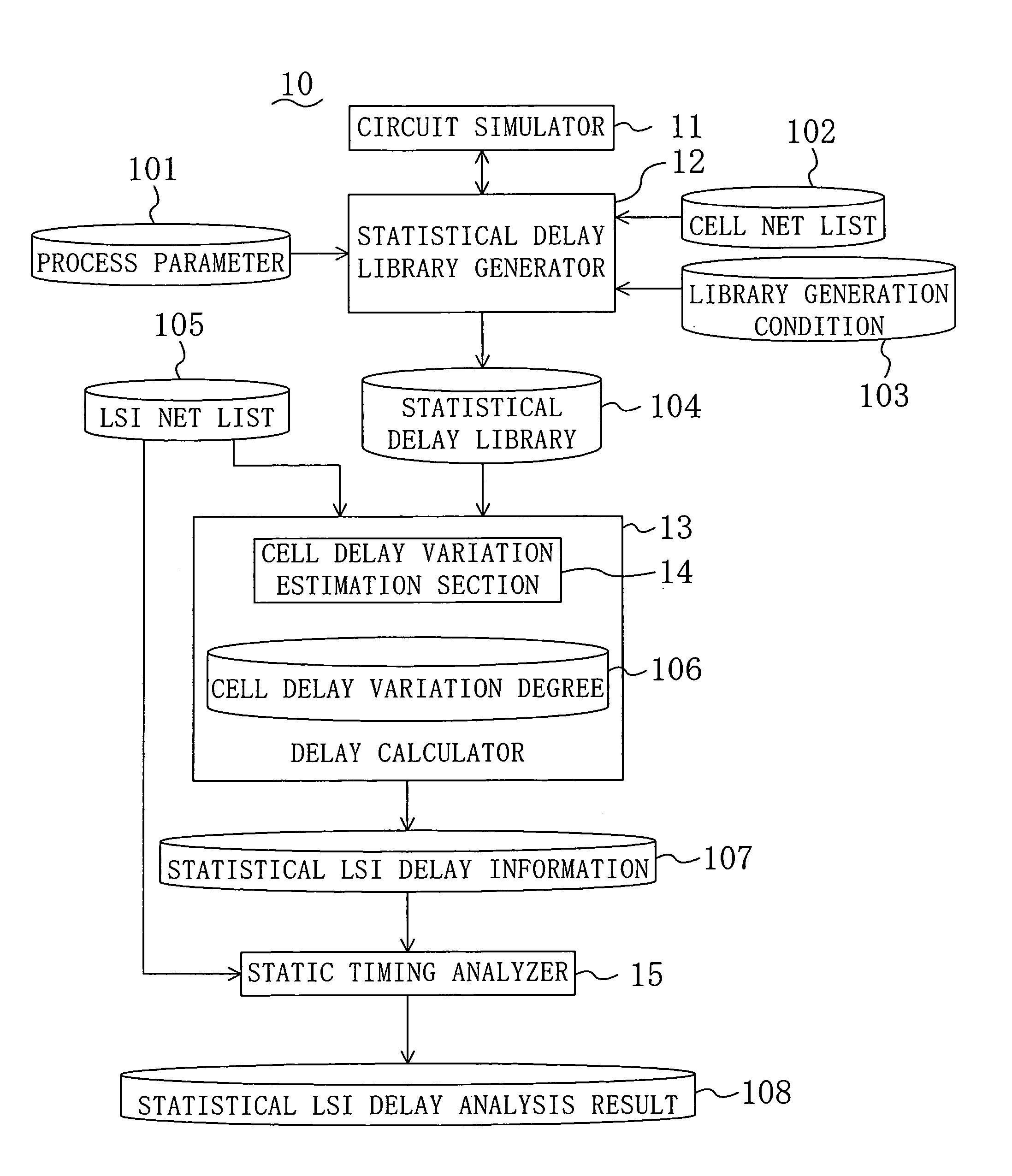
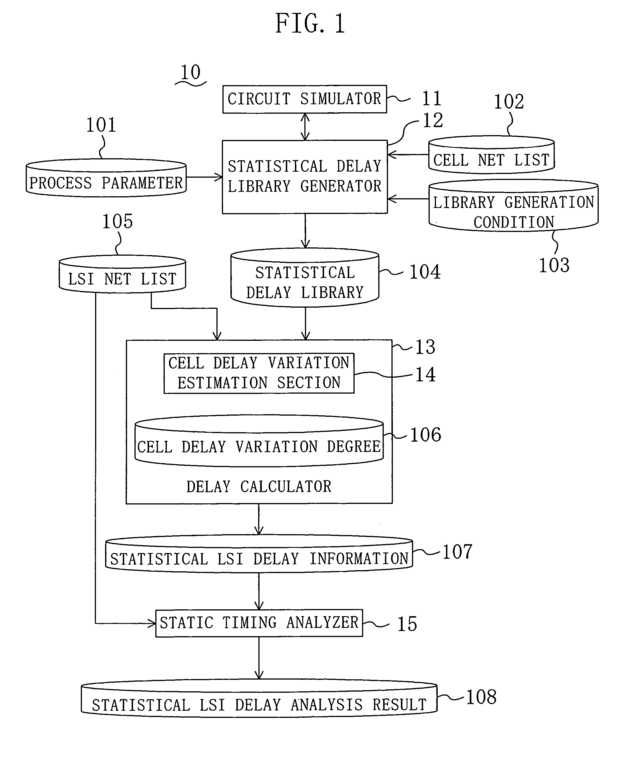
[0064]FIG. 1 is a block diagram illustrating the configuration of a statistical LSI delay simulation apparatus according to a first embodiment of the present invention.

[0065]As shown in FIG. 1, a statistical LSI delay simulation apparatus 10 of this embodiment includes a circuit simulator 11 for simulating the circuit operation of each circuit cell constituting an LSI to be analyzed, a statistical delay library generator 12 for driving the circuit simulator 11 to generate a statistical delay library 104, a delay calculator 13 for calculating a delay amount of each circuit cell in the LSI to be analyzed to generate a statistical LSI delay information file 107 containing delay data for each circuit cell, a static timing analyzer 15 for simulating, based on the data contained in the statistical LSI delay information file 107, the operation of the LSI to be ...

second embodiment

[0134](Second Embodiment)

[0135]Hereinafter, a second embodiment of the present invention will be described with reference to the accompanying drawings.

[0136]FIG. 10 is a block diagram illustrating the configuration of a statistical LSI delay simulation apparatus according to a second embodiment of the present invention. In FIG. 10, each member also shown in FIG. 1 is identified by the same reference numeral, and therefore description thereof will be omitted.

[0137]Unlike the first embodiment, even though a distribution of a variation in delay of a circuit cell is assumed to be a normal distribution, a statistical delay library generator 12A according to the second embodiment does not directly extract a delay average value μ and a delay standard deviation σ by circuit simulation, but extracts a delay average value μ and a delay standard deviation value σ′ (where σ′=σ / μ) normalized with the delay average value μ. In this point, the second embodiment is different from the first embodime...

third embodiment

[0147](Third Embodiment)

[0148]Hereinafter, a third embodiment of the present invention will be described with reference to the accompanying drawings.

[0149]FIG. 13 is a block diagram illustrating the configuration of a statistical LSI delay simulation apparatus according to a third embodiment of the present invention. In FIG. 13, each member also shown in FIG. 1 is identified by the same reference numeral, and therefore description thereof will be omitted.

[0150]Unlike the first embodiment, even though a distribution of a variation of a circuit cell is assumed to be a normal distribution, a statistical delay library generator 12B according to the third embodiment does not directly extract a delay average value μ and a delay standard deviation σ by circuit simulation, but obtains a delay average value μ and then obtains a delay standard deviation value σ from the obtained delay average value μ. In this point, the third embodiment is different from the first embodiment.

[0151]FIG. 14 ill...


PUM


Abstract

A statistical delay simulation apparatus includes: a circuit simulator for simulating a circuit operation of a circuit cell constituting an LSI; a statistical delay library generator for driving the circuit simulator and generating, based on a process parameter and the like, a statistical delay library in which the dependency of a delay variation on a predetermined operation condition in each circuit cell is described; a delay calculator for calculating a delay amount of each circuit cell to generate a statistical LSI delay information file containing data on the calculated delay amount; and a static timing analyzer for simulating, based on data of the statistical LSI delay information file, an operation with a delay variation of the LSI to generate a statistical LSI delay analysis result file.

Description

BACKGROUND OF THE INVENTION[0001]The present invention relates to a statistical simulation apparatus and a simulation method for estimating a variation in delay of an LSI circuit due to variation causes occurring in LSI fabrication processes or the like and utilizing a result of the estimation in simulation of LSI circuit delay.[0002]With development of fabrication technologies, rapid improvements of transistors have been made in terms of size reduction and integration density increase. Accordingly, as for CMIS semiconductor integrated circuit devices (hereinafter, referred to as “LSIs”), devices in which various functions are formed on one chip have been developed in recent years.[0003]When an LSI is developed, a design margin is normally provided during fabrication process steps. There are various factors requiring consideration of a design margin. For example, a variation in electric properties of each transistor constituting a circuit may be caused in fabrication process steps o...

Claims


Application Information

Patent Timeline
IPC IPC(8): G06F17/50G06F17/10
CPCG06F17/5022G06F17/5036G06F2217/10G06F30/33G06F30/367G06F2111/08
Inventor YONEZAWA, HIROKAZU
Owner PANASONIC CORP
Learn More