Apparatus for a differential self-biasing CMOS amplifier

Inactive Publication Date: 2007-06-05
AVAGO TECH INT SALES PTE LTD
View PDF14 Cites 5 Cited by
  • Summary
  • Abstract
  • Description
  • Claims
  • Application Information

AI Technical Summary

Benefits of technology

[0004]FIG. 1 illustrates an exemplary conventional complemen

Problems solved by technology

High swing or high power devices such as, data drivers in a wire line communication system or transmitters in wireless communications systems, may be sources of noise.
The noise may also be caused, for example, by the driving of active circuits.
In another example, noise may be caused by transitions in a signal propagated or generated by the chip.
These errors may include internal or external errors.
Internal errors may include temperature changes, which in certain instances, may affect both sides of the operational amplifier to approximately the same degree.
Transistor mismatch is another example of an internal error.
External errors may include noise picked up by inputs of the differential amplifier.
Additionally, some differential amplifier designs utilize large numbers of transistors.
Consequently, differential amplifiers that utilize a large number of transistors may be more difficult to control and tune, and may also be less predictable with respect to process or operating variations.
These conventional analog differential amplifiers are usually optimized to operate in a specified voltage range and may not function at all if operated outside that range.

Method used


Image

  • Apparatus for a differential self-biasing CMOS amplifier
  • Apparatus for a differential self-biasing CMOS amplifier
  • Apparatus for a differential self-biasing CMOS amplifier

Examples


Embodiment Construction

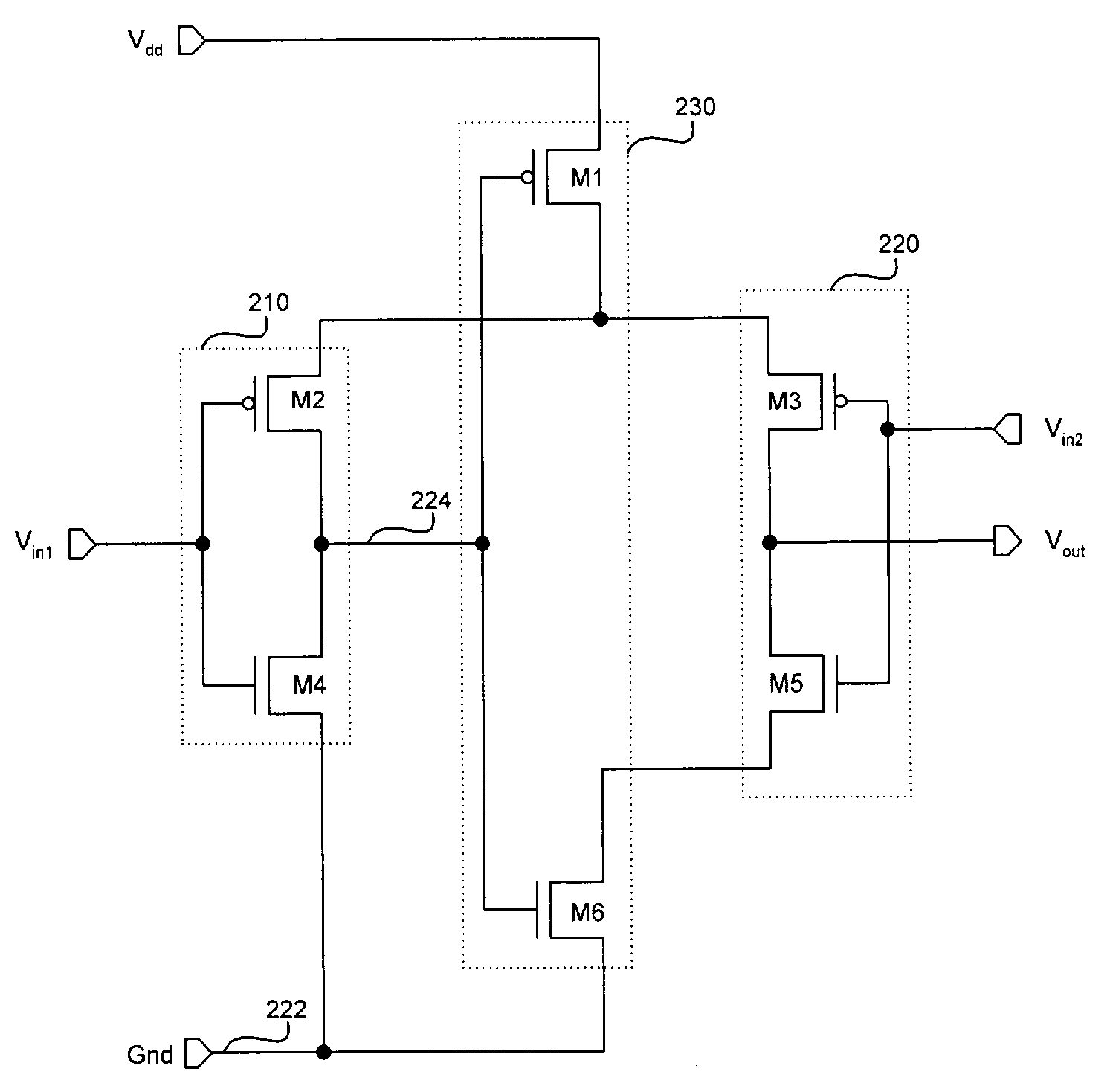
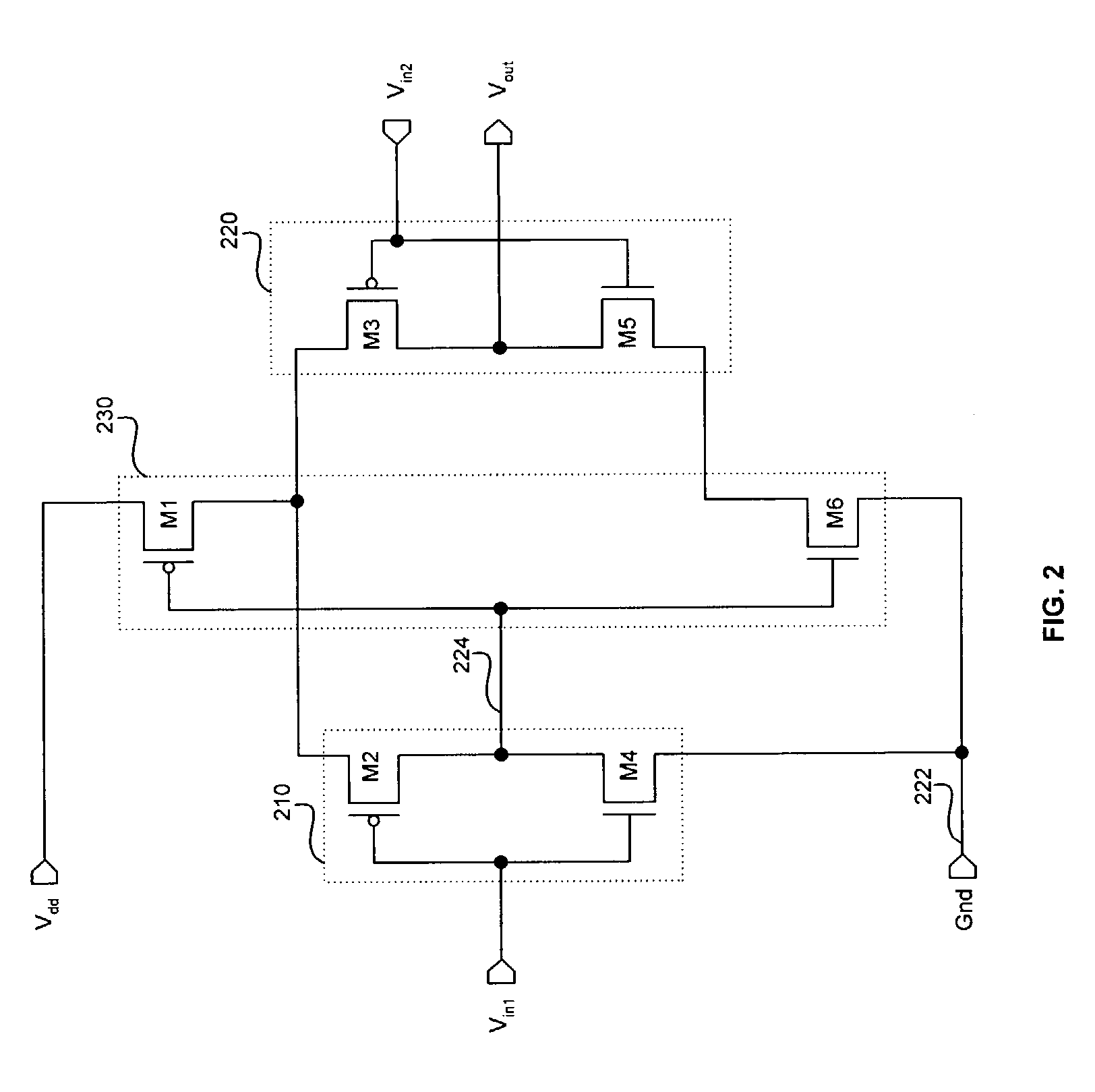
[0019]Aspects of the invention provide a self-biasing differential amplifier. The self-biasing differential amplifier may include a first input stage and a biasing transistor pair coupled to the first input stage. A second input stage may be coupled to the first input stage and the biasing transistor pair. The first input stage of the self-biasing differential amplifier may include a first PMOS transistor coupled to a first NMOS transistor in an inverter arrangement. The second input stage may include a second PMOS transistor coupled to a second NMOS transistor. The biasing transistor pair may include a third PMOS transistor coupled to a third NMOS transistor.

[0020]The self-biasing differential amplifier in accordance with an embodiment of the invention is in a class of differential amplifier designs that may be implemented with relatively few transistors making it very compact and flexible. The self-biasing differential amplifier does not require any other reference voltage or refe...


PUM


Abstract

Aspects of the invention provide a self-biasing differential amplifier. The self-biasing differential amplifier may include a first input stage and a biasing transistor pair coupled to the first input stage. A second input stage may be coupled to the first input stage and the biasing transistor pair. The first input stage of the self-biasing differential amplifier may include a first PMOS transistor coupled to a first NMOS transistor in an inverter arrangement. The second input stage may include a second PMOS transistor coupled to a second NMOS transistor. The biasing transistor pair may include a third PMOS transistor coupled to a third NMOS transistor.

Description

CROSS-REFERENCE TO RELATED APPLICATIONS / INCORPORATION BY REFERENCE[0001]Not Applicable.FIELD OF THE INVENTION[0002]Certain embodiments of the invention relate to differential amplifiers. More specifically, certain embodiments of the invention relate to an apparatus for a self-biasing or self-referencing differential amplifier.BACKGROUND OF THE INVENTION[0003]A transistor is an electronic device that permits current flow in electronic circuits. In this regard, the transistor permits the current to flow in a controlled manner whenever an electronic circuit attempts to push current through the transistor. In this manner, the transistor generically operates as a regulator or valve, which regulates the flow of current.[0004]FIG. 1 illustrates an exemplary conventional complementary metal oxide semiconductor (CMOS) transistor arrangement. Referring to FIG. 1, the conventional CMOS transistor arrangement 24 includes an n-channel MOS (NMOS) transistor 18 and a p-channel MOS (PMOS) transisto...

Claims


Application Information

Patent Timeline
IPC IPC(8): H03F3/45
CPCH03F3/45179H03F3/45237
Inventor SLAMOWITZ, MARK
Owner AVAGO TECH INT SALES PTE LTD
Why Eureka
Try Eureka