Octagonal interconnection network for linking processing nodes on an SOC device and method of operating same

Inactive Publication Date: 2007-05-15
STMICROELECTRONICS SRL
View PDF5 Cites 13 Cited by
  • Summary
  • Abstract
  • Description
  • Claims
  • Application Information

AI Technical Summary

Benefits of technology

[0018]To address the above-discussed deficiencies of the prior art, it is a primary object of the present invention to provide an improved interconnection network for routing data packets. According to an advantageous embodiment of the present invention, the interconnection network comprises: 1) eight switching circuits capable of transferring data packets with each other; 2) eight sequential data links bidirectionally coupling the eight switching circuits in sequence to thereby form an octagonal

Problems solved by technology

This will have a dramatic effect on the complexity and protocols of communication networks.
However, it is becoming apparent that traditional SOC devices and processors cannot keep up with the speed and programmability requirements of evolving networks.
If a data packet processing engine is unable to continue work because it is limited by a slow interconnection network in the network processing unit (NPU), then much of the processing power is wasted.
A primary source of delay in the interconnection network in a network processing unit (NPU) and many other system-on-a-chip (SOC) devices is the number of data links that a data packet must traverse to get from a source node to a destination node within the NPU or other SOC device.
Unfortunately, eliminating all multiple hop data links by connecting all processing nodes directly to all other processing nodes, such as by means of an N×N crossbar, results in a complex interconnection network that reduces the speed of data transfers due to the physical length of the interconnections and interference between the interconnections.

Method used


Image

  • Octagonal interconnection network for linking processing nodes on an SOC device and method of operating same
  • Octagonal interconnection network for linking processing nodes on an SOC device and method of operating same
  • Octagonal interconnection network for linking processing nodes on an SOC device and method of operating same

Examples


Embodiment Construction

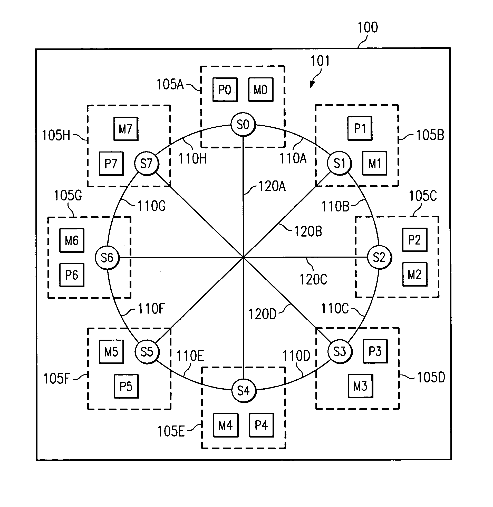
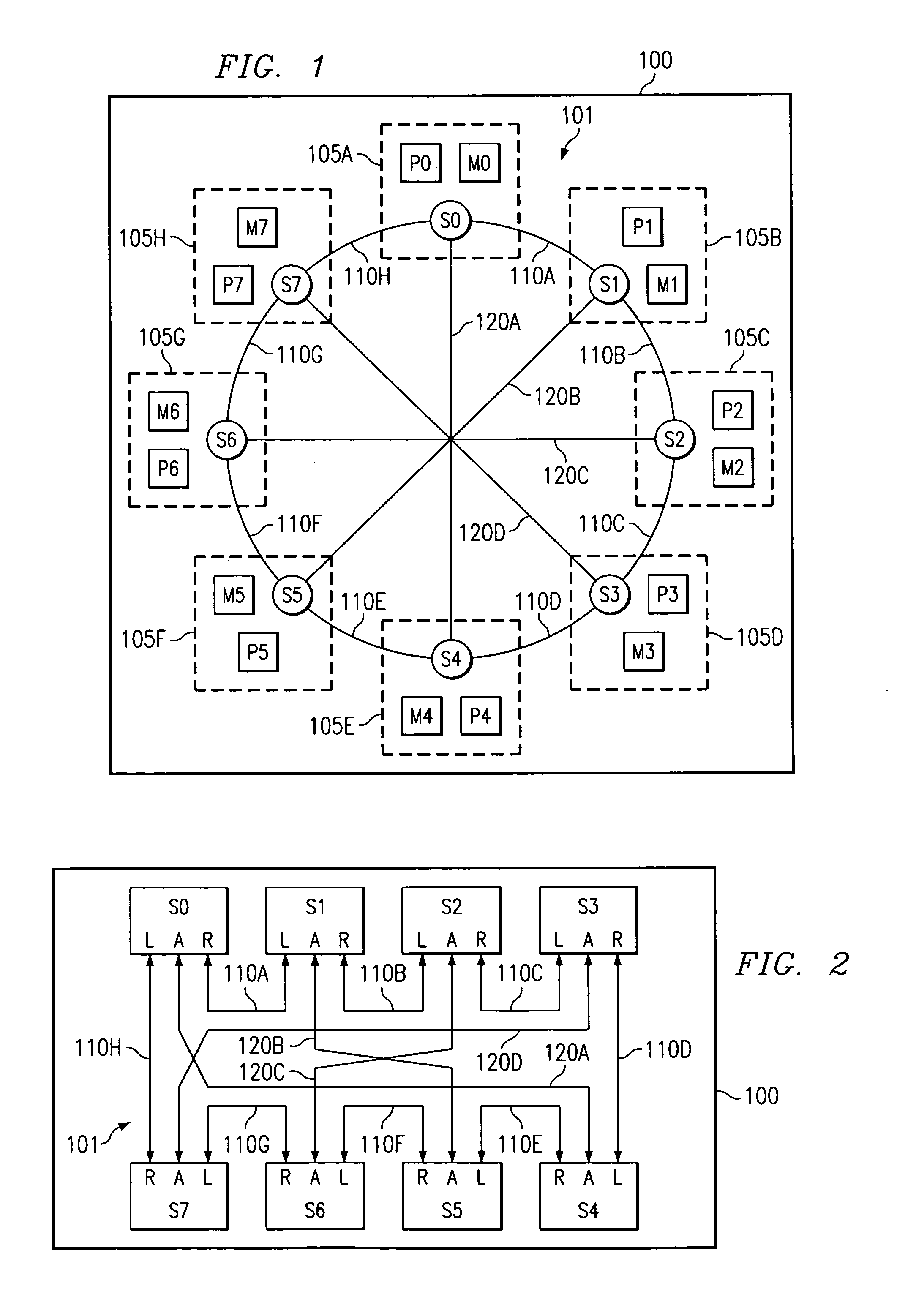
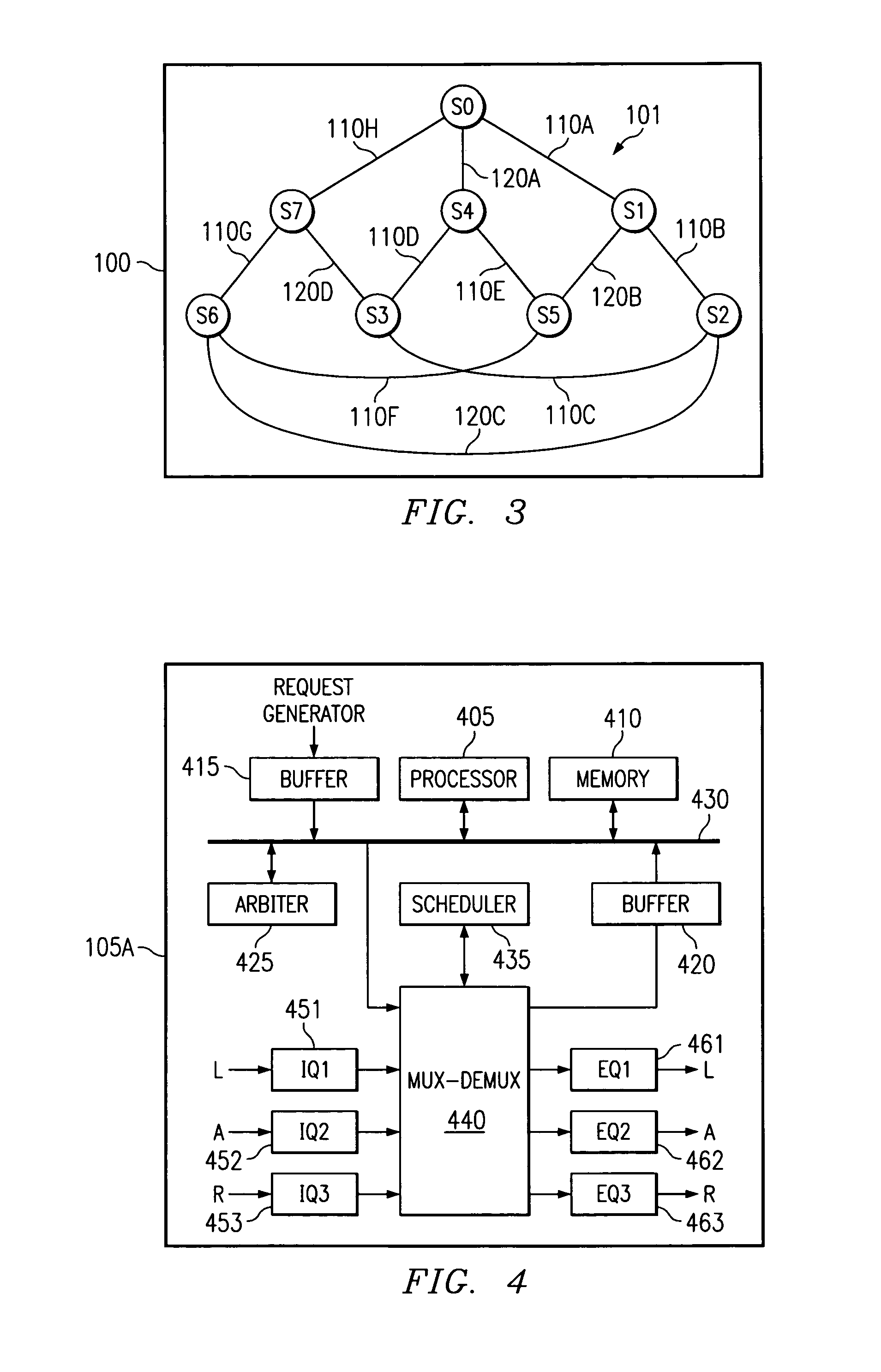
[0035]FIGS. 1 through 6, discussed below, and the various embodiments used to describe the principles of the present invention in this patent document are by way of illustration only and should not be construed in any way so as to limit the scope of the invention. Those skilled in the art will understand that the principles of the present invention may be implemented in any suitably arranged system-on-a-chip (SOC) device.

[0036]FIG. 1 illustrates exemplary system-on-a-chip (SOC) device 100, which contains an octagonal interconnection network (generally designated “101”) according to the principles of the present invention. SOC device 100 comprises eight processing nodes 105A–105H. Each processing node 105 comprises a processor (Pi), a memory (Mi), and switching (or routing) circuit (Si) that forms a portion of octagonal interconnection network 101. Each processing node may comprise additional peripheral circuitry (not shown) coupled to the processor and the memory. For example, proce...


PUM


Abstract

An octagonal interconnection network for routing data packets. The interconnection network comprises: 1) eight switching circuits for transferring data packets with each other; 2) eight sequential data links bidirectionally coupling the eight switching circuits in sequence to thereby form an octagonal ring configuration; and 3) four crossing data links, wherein a first crossing data link bidirectionally couples a first switching circuit to a fifth switching circuit, a second crossing data link bidirectionally couples a second switching circuit to a sixth switching circuit, a third crossing data link bidirectionally couples a third switching circuit to a seventh switching circuit, and a fourth crossing data link bidirectionally couples a fourth switching circuit to an eighth switching circuit.

Description

[0001]The present invention claims priority to 1) U.S. Provisional Patent Application Ser. No. 60 / 274,422, filed Mar. 9, 2001; and 2) U.S. Provisional Patent Application Ser. No. 60 / 309,739, filed Aug. 2, 2001.CROSS-REFERENCE TO RELATED APPLICATIONS[0002]The present invention is related to those disclosed in:[0003]1) U.S. Provisional Patent Application Ser. No. 60 / 274,422, filed Mar. 9, 2001, entitled “NETWORK OF PROCESSING NODES ON A CHIP AND METHOD OF OPERATING THE SAME”; and[0004]2) U.S. Provisional Patent Application Ser. No. 60 / 309,739, filed Aug. 2, 2001, entitled “ON-CHIP COMMUNICATION ARCHITECTURE FOR OC-768 NETWORK PROCESSORS”.[0005]Provisional Patent Application Ser. Nos. 60 / 274,422 and 60 / 309,739 are commonly assigned to the assignee of the present invention. The disclosures of the related provisional applications are hereby incorporated by reference for all purposes.TECHNICAL FIELD OF THE INVENTION[0006]The present invention is generally directed to system-on-a-chip (SOC...

Claims


Application Information

Patent Timeline
IPC IPC(8): H04L12/56G06F13/36H04L12/28H04L12/42H04L12/66
CPCH04L49/109H04L49/15H04L49/352H04L49/357
Inventor KARIM, FARAYDON O.
Owner STMICROELECTRONICS SRL
Why Eureka
Try Eureka