
High-stability shift circuit using amorphous silicon thin film transistors

a technology shift circuits, applied in static storage, digital storage, instruments, etc., can solve the problems of increasing the number of the complexity of the manufacturing process and the electrical characteristics, and the increase of the tft elements that follow the affection of bias stress, etc., to reduce the shift of threshold voltage, increase the lifetime of amorphous silicon thin film transistors, and increase the operating time

Active Publication Date: 2007-04-10
WINTEK CORP
View PDF4 Cites 86 Cited by
  • Summary
  • Abstract
  • Description
  • Claims
  • Application Information

AI Technical Summary

Benefits of technology

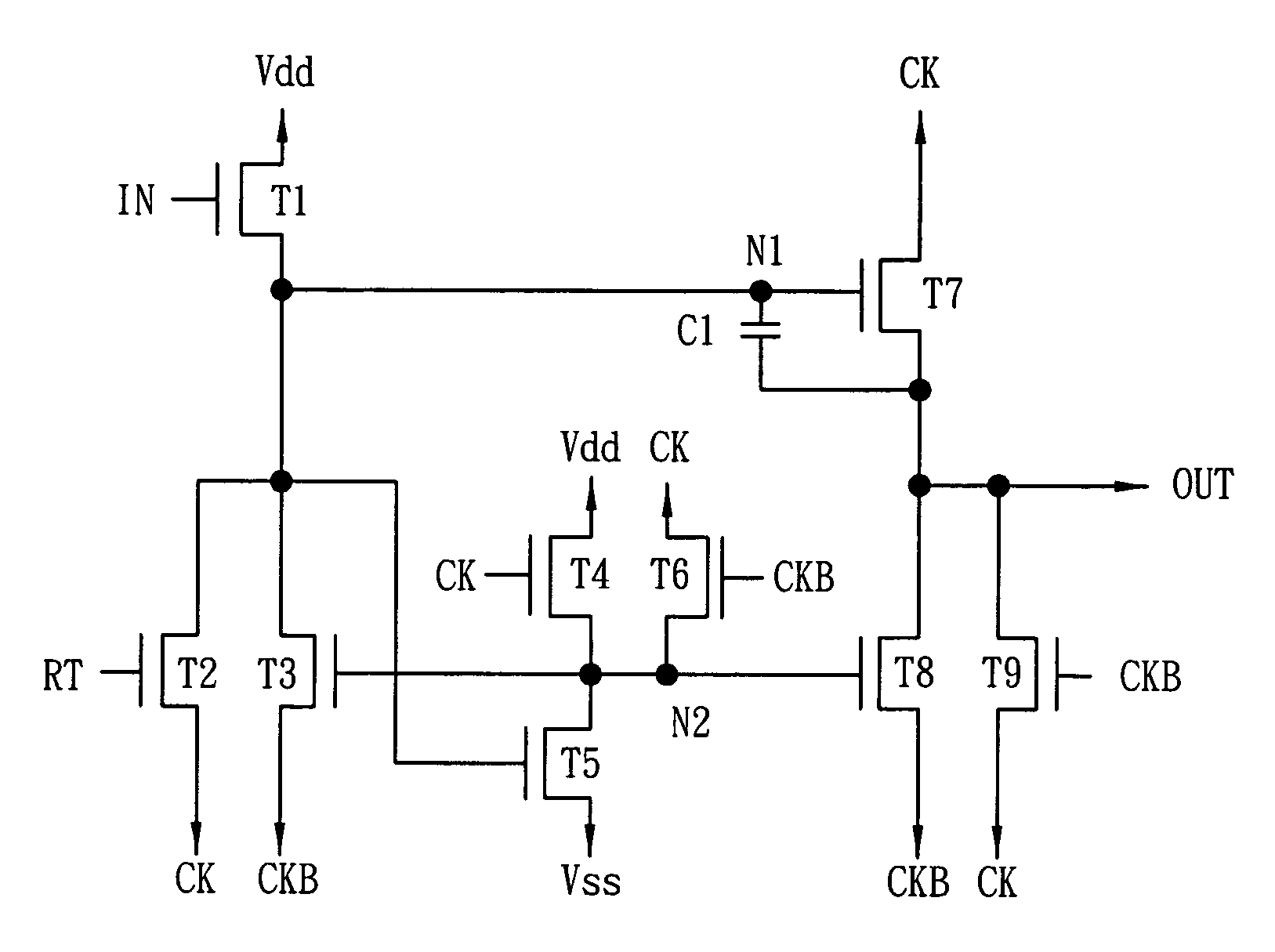
[0008]Consequently, the main purpose of the current invention is to add a recovery mechanism for restraining the threshold voltage shift of the a-Si TFTs by the innovative circuit so as to avoid that the a-Si TFTs affect the scanning signal of the shift register due to the threshold voltage shift.
[0009]Another purpose of the current invention is to reduce the extent of the threshold voltage shift of the a-Si TFTs by using the aforementioned recovery mechanism so as to promote the stability of the scanning shift circuit, to increase the lifetime of the a-Si TFTs, and to extend the operating time of the shift circuit.
[0015]By this, when the two out-of-phase signals: the first clock-pulse and the second clock-pulse are fed into the shift circuit of this invention, the driving conditions for the third, eighth, and ninth transistor are positive / negative-alternating biases. The positive / negative-alternating biases can restrain the shift of the threshold voltage such that the threshold voltage of the transistor will not excessively increase along with the increasing operating time. Accordingly, this can not only increase the lifetime of the amorphous silicon thin film transistors, extend the operating time of the shift circuit, but also can avoid that the a-Si TFTs affect the scanning signal of the whole shift register due to the threshold voltage shift.

Problems solved by technology

The major difference between a LTPS TFT and an a-Si TFT is the complexity of the manufacturing process and the electrical characteristics.
A LTPS TFT has a higher carrier-mobility whereas its manufacturing process is more complicated.
However, due to the limit of manufacturing ability, the threshold voltage (Vth) for the manufactured a-Si TFT elements that follows the affection of the bias stress increases gradually.
Along with the increasing operating time, the Vth shift severely affects the normal operation of the scanning shift circuit, even the scanning shift circuit will fail at last.
As a result, the output terminal OUT is easily affected by other signals or noises such that the output terminal OUT cannot be kept at a low-level state (VSS).

Method used


Image

  • High-stability shift circuit using amorphous silicon thin film transistors
  • High-stability shift circuit using amorphous silicon thin film transistors
  • High-stability shift circuit using amorphous silicon thin film transistors

Examples


Embodiment Construction

[0024]The detailed descriptions for content and technology of this invention associate with figures are as follows.

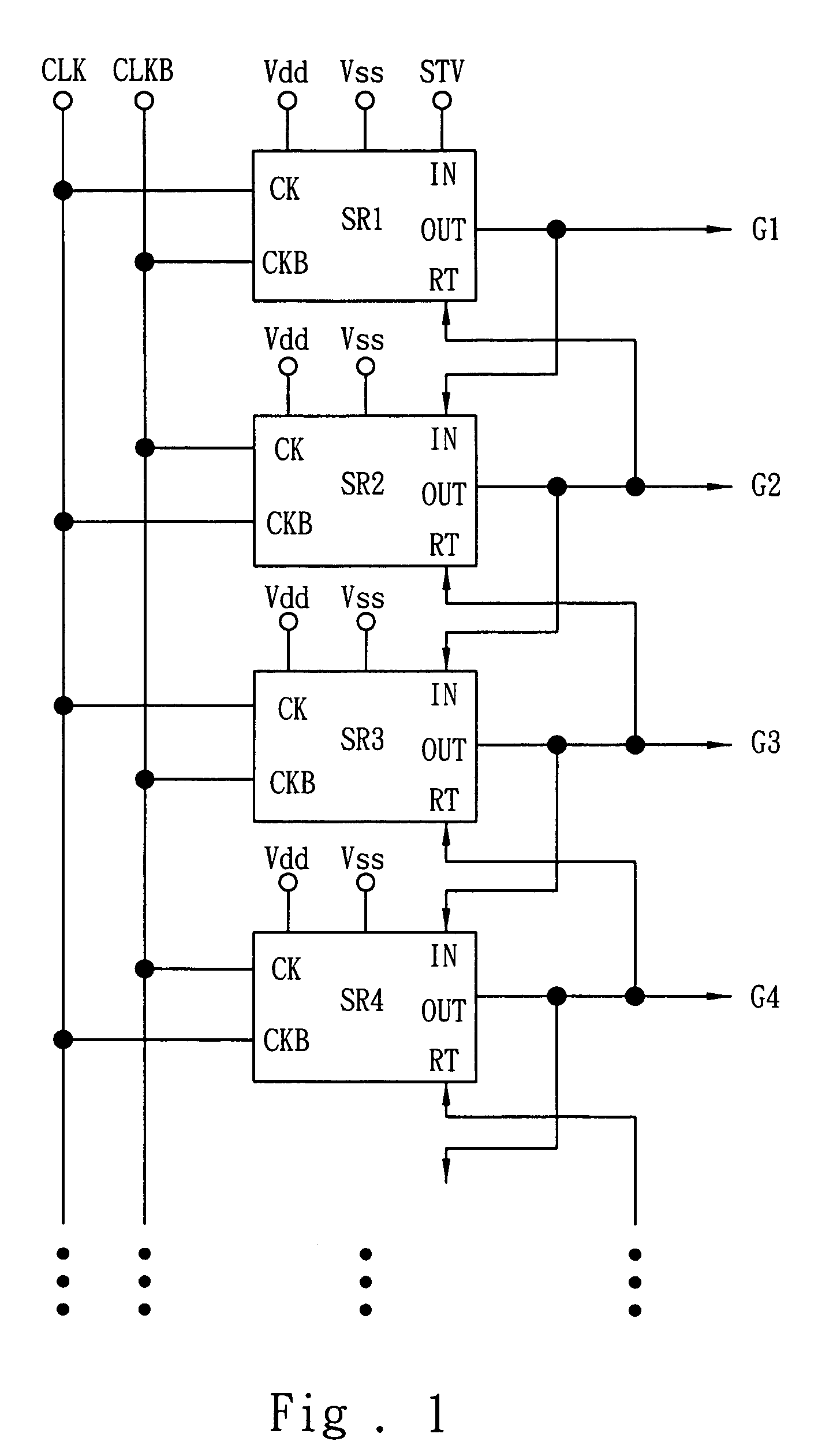
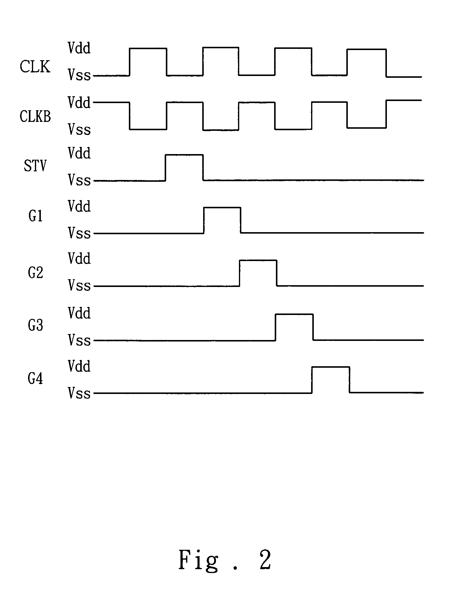
[0025]Please refer to FIGS. 1 and 2, which are the block diagram and the timing diagram for the output and input signals, respectively, for the shift register of the current invention. As shown in the figures, the present invention is applied to shift register circuits that are composed of amorphous silicon thin film transistors. The invention is a scanning driving circuit that can be integrated to a glass substrate. The shift register of this invention is composed of several stages. The stages are connected in serial and send the output signals G1, G2, G3, G4, . . . to the gate lines in the panel. The two power sources are a high-level supply voltage Vdd and a low-level supply voltage Vss. The input signals include the first clock-pulse signal CLK and the second clock-pulse signal CLKB, they are out-of-phase to each other, and the start signal STV.

[0026]Initially, a se...


PUM


Abstract

A high-stability shift circuit using amorphous silicon thin film transistors, which utilizes two out-of-phase pulses to control the operating mechanism and the bias-relations among transistors in the shift circuit. This makes the transistors under the driving conditions of positive / negative-alternating biases so as to restrain the voltage shift of the transistors such that the threshold voltage will not excessively increase along with the increasing operating time. This can not only increase the lifetime of the amorphous silicon thin film transistors but also extend the operating time of the shift circuit.

Description

FIELD OF THE INVENTION[0001]The present invention relates to a scanning shift circuit whose components are amorphous silicon thin film transistors. This shift circuit has the mechanism for restraining the threshold voltage shift of the amorphous silicon thin film transistors, reducing the extent of the threshold voltage shift, so as to increase the stability of the scanning shift circuit and to extend the lifetime of the shift circuit.BACKGROUND OF THE INVENTION[0002]In recent years, the technology of thin film transistor panel is making progress continuously, which includes the driving circuit been integrated on panels. Such as the SOG (system on glass) technology can be actualized by technologies of a-Si (amorphous silicon) and LTPS (low temperature poly-silicon). The major difference between a LTPS TFT and an a-Si TFT is the complexity of the manufacturing process and the electrical characteristics. A LTPS TFT has a higher carrier-mobility whereas its manufacturing process is mor...

Claims


Application Information

Patent Timeline
Patent Type & Authority Patents(United States)
IPC IPC(8): G11C19/00
CPCG11C19/28
Inventor LO, SHIN-TAILIN, YI-CHINWENG, RUEY-SHING
Owner WINTEK CORP
Learn More