Semiconductor memory

a semiconductor memory and memory technology, applied in the field of semiconductor memory, can solve the problems of degradation (delay) in data output time or access time, difficult to obtain a reference voltage in the finished chip, and different reference voltages in the simulation, etc., and achieve the effect of shortening access time and increasing the area of semiconductor memory

Inactive Publication Date: 2007-03-27
RENESAS ELECTRONICS CORP
View PDF8 Cites 12 Cited by
  • Summary
  • Abstract
  • Description
  • Claims
  • Application Information

AI Technical Summary

Benefits of technology

[0024]In view of the foregoing, it is an object of the present invention to provide a semiconductor memory that outputs data at high-speed to allow shorter access time, preferably without increasing the area of the semiconductor memory.
[0036]A semiconductor memory according to the present invention has a plurality of dummy cells with different current capacities to generate a plurality of levels of reference voltages, and selectively uses an appropriate reference voltage which is a center level between High level and Low level of memory cell data. It is thus possible to achieve high-speed data output time and a shorter access time.
[0037]Further, each dummy cell generates a reference voltage based on a drive signal via a common dummy word line, that is, each dummy cell is driven by a single dummy word line, thereby eliminating a need for forming a plurality of rows of dummy cells. It is thus possible to achieve a target reference voltage without increasing the area of the semiconductor memory.

Problems solved by technology

However, a reference voltage in a finished chip can be different from a simulation result at the time of design.
It is thereby difficult to obtain a reference voltage in a finished chip having a center level between High and Low levels of memory cell data (digit voltage).
If the reference level is not the center level, a difference between the reference voltage and the digit voltage becomes undesirably small to cause degradation (delay) in data output time or access time.
A difference between High level of the digit voltage and the reference level thereby becomes small, causing delay in output time of High level data.
A difference between Low level of the digit voltage and the reference level thereby becomes small, causing delay in output time of Low level data.
However, in the case where the reference level is higher than the center level as shown in FIG. 12, an elapsed time until the difference S reaches a predetermined level is delayed when the memory cell data is High, causing a delay in data output timing.
On the other hand, in the case where the reference level is lower than the center level as shown in FIG. 13, an elapsed time until the difference S reaches a predetermined level is delayed when the memory cell data is Low, causing a delay in data output timing.
In this way, if the reference level is not the center level, output timing of High or Low level data is delayed, which hinders high-speed data output as simulated at the time of design.

Method used


Image

  • Semiconductor memory
  • Semiconductor memory
  • Semiconductor memory

Examples


Embodiment Construction

[0052]Preferred embodiments of the present invention are explained hereinafter with reference to the drawings. A semiconductor memory and its reference voltage generation method are described in the following embodiments.

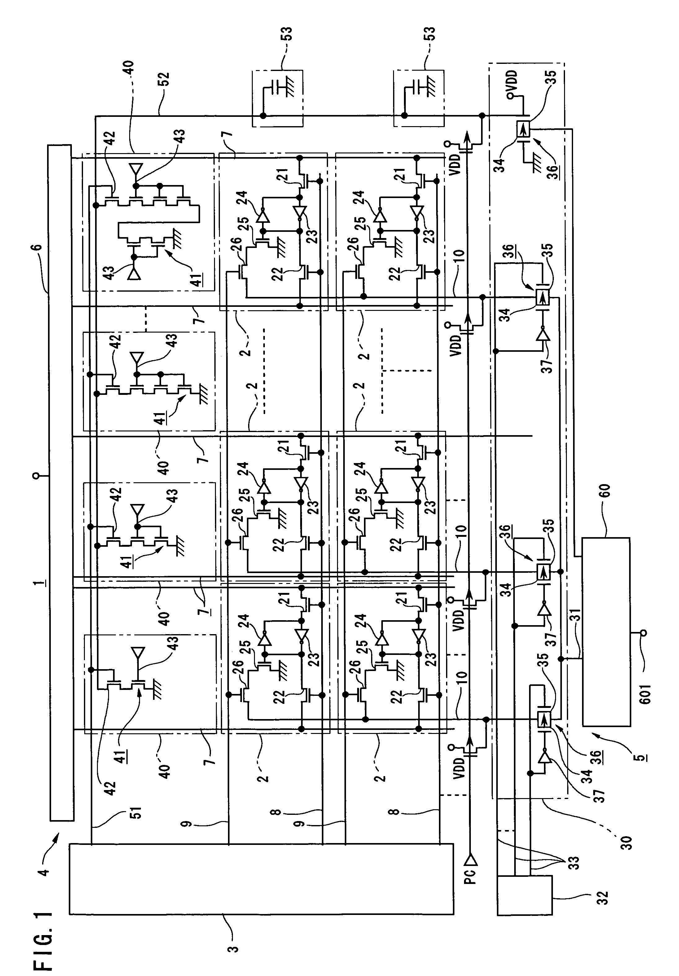
[0053]FIG. 1 illustrates a circuit in the vicinity of a memory cell of a semiconductor memory 1 according to a specific embodiment of the present invention.

[0054]The semiconductor memory 1 of this embodiment is SRAM, for example, and it has an array of memory cells 2 composed of the n-number of rows and them-number of columns, thus having n×m bits, a word line driver circuit 3 used for both write and read operation, a write-only port 4, and a read-only port 5.

[0055]The write-only port 4 has a known structure, for example, having a data write buffer 6 for temporarily buffering inputted write data and outputting the data, write digit lines 7 complementarily provided two lines for each column for transmitting data write signal outputted from the data write buffer 6, an...


PUM


Abstract

A semiconductor memory has a plurality of memory cells having a single-ended digit structure. When reading data from a selected memory cell, a digit voltage outputted from the selected memory cell is compared with a reference voltage. If the digit voltage is higher, it is outputted as High level; if the digit voltage is lower, it is outputted as Low level. The semiconductor memory further has a plurality of dummy cells with different current capacity to generate a plurality of different levels of reference voltages.

Description

BACKGROUND OF THE INVENTION[0001]1. Field of the Invention[0002]The present invention relates to a semiconductor memory having a memory cell with a single-ended digit structure that reads data over a single digit line.[0003]2. Description of Related Art[0004]A semiconductor memory having a memory cell with a single-ended digit structure, as shown in FIG. 10, for example, is widely known. Japanese Unexamined Patent Application Publication No. 03-73493 (FIG. 2), for example, describes this kind of semiconductor memory.[0005]The semiconductor memory 100 shown in FIG. 10 is Static Random Access Memory (SRAM). The semiconductor memory 100 has memory cells 101 arranged in an array composed of the n-number of rows and the m-number of columns (n and m are each positive integers of 2 and above), with n×m bits, and a word line driver circuit 102. Write word lines 103 and read word lines 104, each of the same number as rows (n-number), are derived from the word line driver circuit 102. The in-...

Claims


Application Information

Patent Timeline
Patent Type & Authority Patents(United States)
IPC IPC(8): G11C16/04G11C11/419G11C11/41
CPCG11C11/419
Inventor KATO, TATSUHIRO
Owner RENESAS ELECTRONICS CORP
Why Eureka
Try Eureka