Design layout preparing method
a design layout and preparing method technology, applied in the field of design layout preparing method and system, can solve the problems of difficult to faithfully form a pattern in individual processes, incomplete final processing pattern shape, and complicated design rule (dr) closely relating with the op
- Summary
- Abstract
- Description
- Claims
- Application Information
AI Technical Summary
Benefits of technology
Problems solved by technology
Method used
Image
Examples
first embodiment
[0028](First Embodiment)
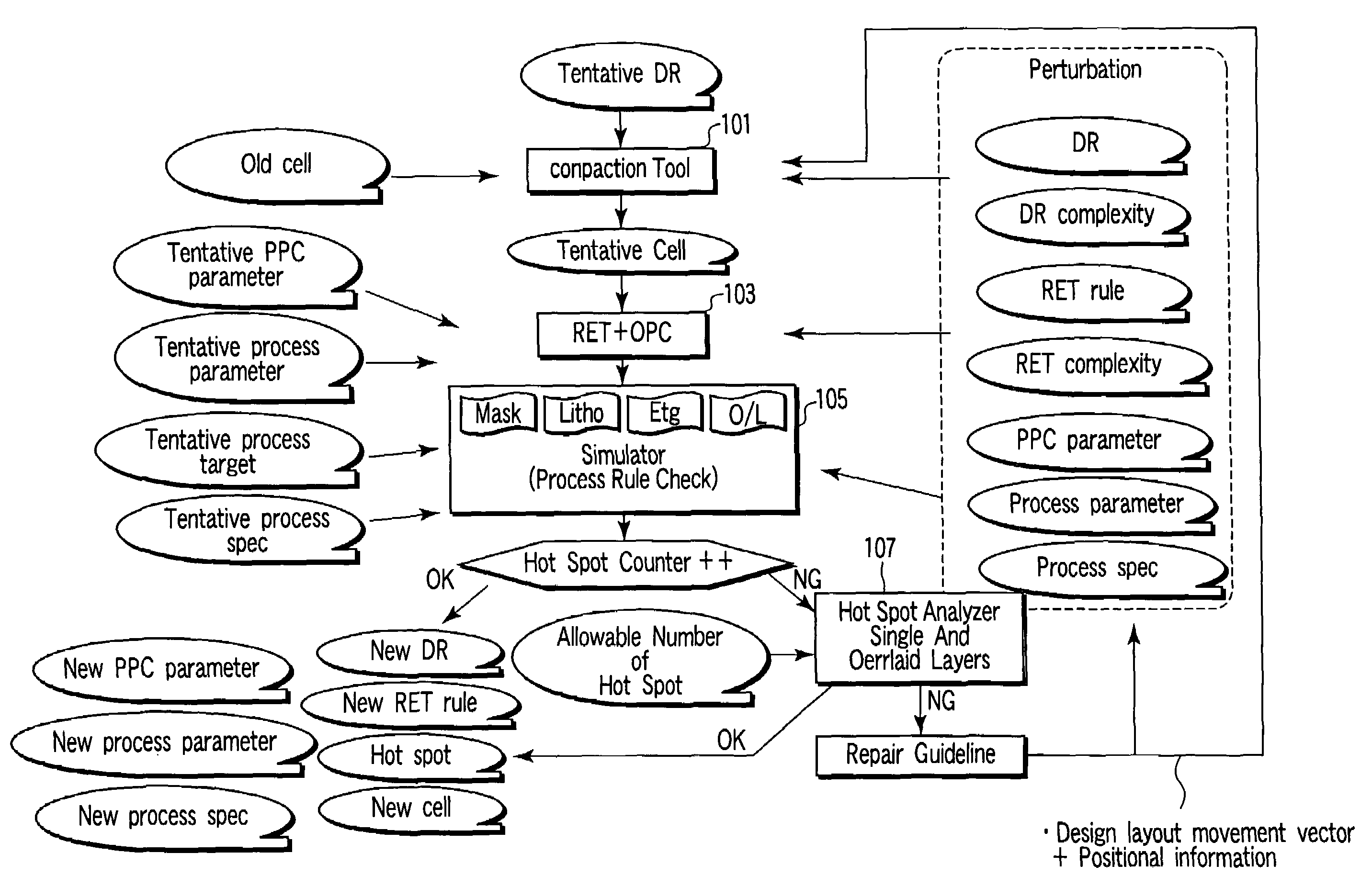
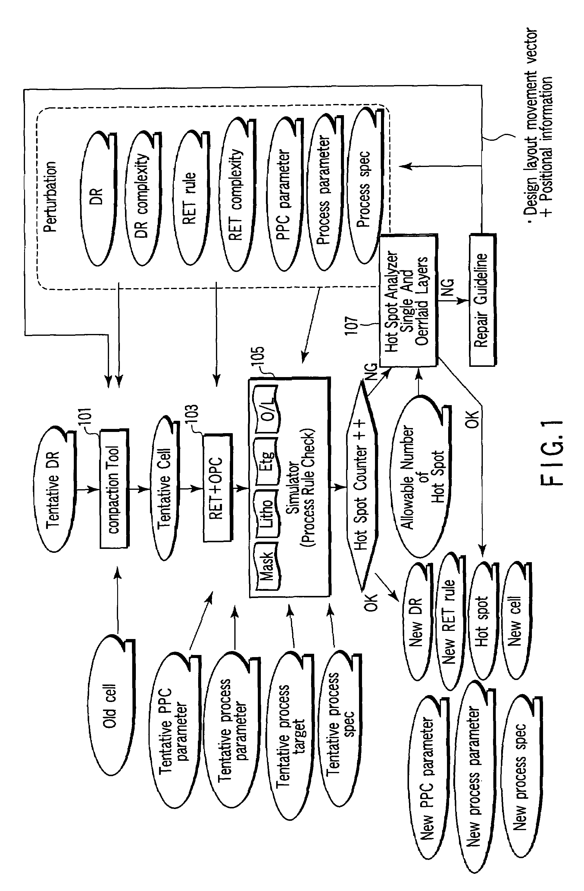
[0029]FIG. 1 is a flowchart to explain the flow of a design layout preparing method according to a first embodiment of the present invention.
[0030]Tentative design rule and layout data are input to a compaction tool 101. In this case, an old-generation standard cell (old cell) is used as layout data. The compaction tool 101 repairs the input layout data so as to satisfy a given design rule (DR). Thus, output layout data (tentative cell) is layout data satisfying the input DR.
[0031]A RET+OPC processing section 103 carries out RET (Resolution Enhancement Technique) processing applied to the foregoing generation with respect to the layout data. The RET processing includes pattern generation processing, pattern delete processing and pattern sort processing. More specifically, the RET processing includes the following processing. One is shifter pasting processing for giving light transmittance and phase to layout data. Another is auxiliary pattern (SRAF: sub-resol...
second embodiment
[0064](Second Embodiment)
[0065]The pattern repair based on the flow described in the first embodiment was carried out with respect to an actual layout. The following is a description of the results.
[0066]Under the process condition that the minimum pattern width is 63 nm, and k1=0.3, exposure dose and focus value are varied, and then, a processed pattern shape on a wafer was calculated. More specifically, three (3) conditions are given as the exposure dose, and two (2) conditions were given as the focus. Then, a processed pattern shape was calculated with respect to each of 6 (=3×2) conditions. FIG. 4(a) is a view showing a state that these processed pattern shapes are overlapped. In FIG. 4(a), a hot spot such that an open / short error is predicted appears in portions surrounded by a circle.
[0067]Two values were calculated from the result shown in FIG. 4(a). FIG. 4(b) shows a distribution of the difference (dispersion) between maximum and minimum values of dimension shift generated u...
PUM
| Property | Measurement | Unit |
|---|---|---|
| dispersion | aaaaa | aaaaa |
| peripheral length | aaaaa | aaaaa |
| wavelength | aaaaa | aaaaa |
Abstract
Description
Claims
Application Information
 - R&D
- Intellectual Property
- Life Sciences
- Materials
- Tech Scout
- Unparalleled Data Quality
- Higher Quality Content
- 60% Fewer Hallucinations
Browse by: Latest US Patents, China's latest patents, Technical Efficacy Thesaurus, Application Domain, Technology Topic, Popular Technical Reports.
© 2025 PatSnap. All rights reserved.Legal|Privacy policy|Modern Slavery Act Transparency Statement|Sitemap|About US| Contact US: help@patsnap.com


